Output buffer with time varying source impedance for driving capacitively-terminated transmission lines

a capacitively-terminated transmission line and output buffer technology, applied in the direction of transmission, logic circuit, electric pulse generator, etc., can solve the problems of data signal distortion, impedance mismatch, transmission line and load impedance equalization, etc., to mitigate the effect of wave reflection

Active Publication Date: 2005-12-27
MARVELL ASIA PTE LTD
View PDF3 Cites 92 Cited by
  • Summary
  • Abstract
  • Description
  • Claims
  • Application Information

AI Technical Summary

Benefits of technology

[0010]The low-Z source impedance during the first and second waveform portions increases the initial voltage delivered into the transmission line (when compared with a standard Z0 source impedance), thereby causing the capacitive load to receive a larger incident pulse such that it is quickly charged, which increases the slew rate at the capacitive load. To mitigate the effect of the wave reflected by the load, the duration of the first and second portions is preferably made less than the twice the data bit's transit time on the transmission line, such that the output impedance Z2 (preferably=Z0) associated with the fourth portion is in place to absorb and / or dissipate the reflected wave and thereby reduce the data signal distortion that might otherwise occur. Overshoot and undershoot problems are also reduced, as the absorption of the reflected wave by Z2 and the lower voltage fourth waveform portion tend to reduce the magnitude of any ringing on the transmission line.

Problems solved by technology

However, it is often impossible to make the transmission line and load impedances equal.
However, the capacitance at the end of the transmission line shunts out the load resistance at higher frequencies, resulting in an impedance mismatch; consequently, with a capacitive load impedance the data signal transition is at least partially reflected back towards the source.
However, a low output impedance tends to maximize the magnitude of the signal reflected by the source back towards the load, and thus the data signal distortion.
However, this approach requires complex look-ahead and output voltage adjustment circuitry, which does nothing to reduce the magnitude of the reflected waves, or to address their causes.

Method used


Image

  • Output buffer with time varying source impedance for driving capacitively-terminated transmission lines
  • Output buffer with time varying source impedance for driving capacitively-terminated transmission lines
  • Output buffer with time varying source impedance for driving capacitively-terminated transmission lines

Examples


Embodiment Construction

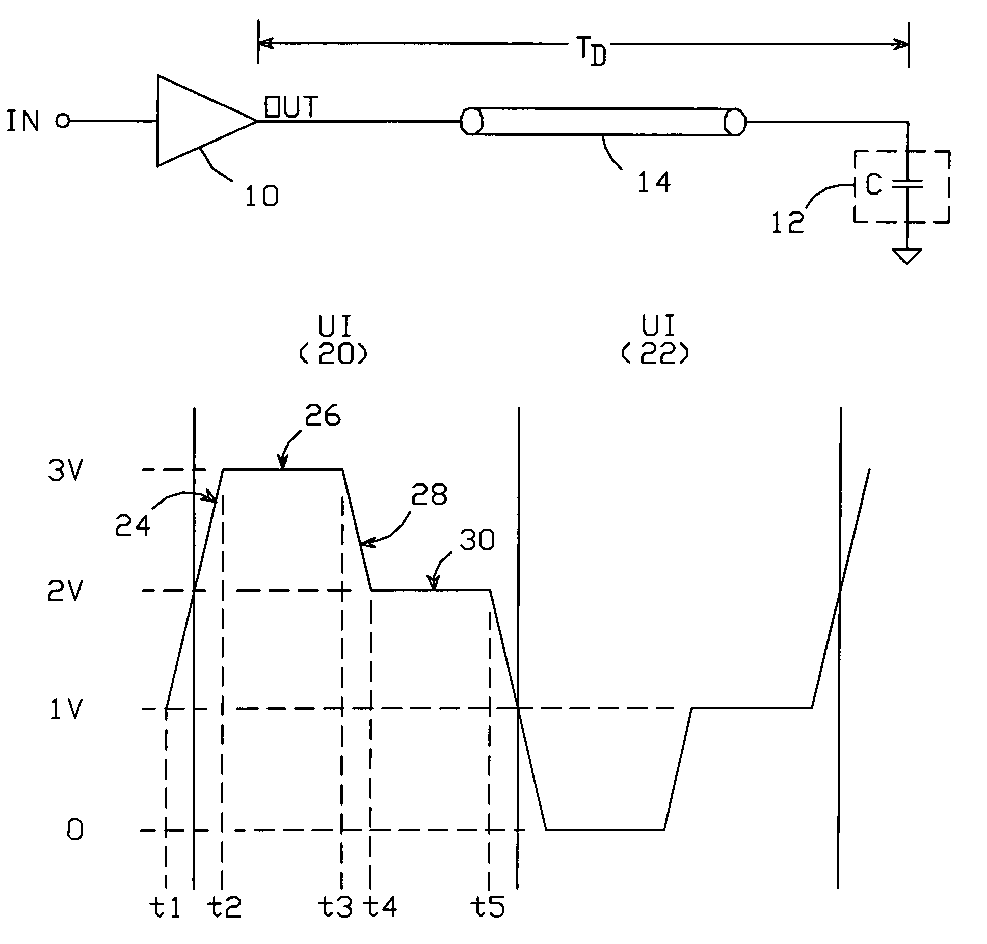
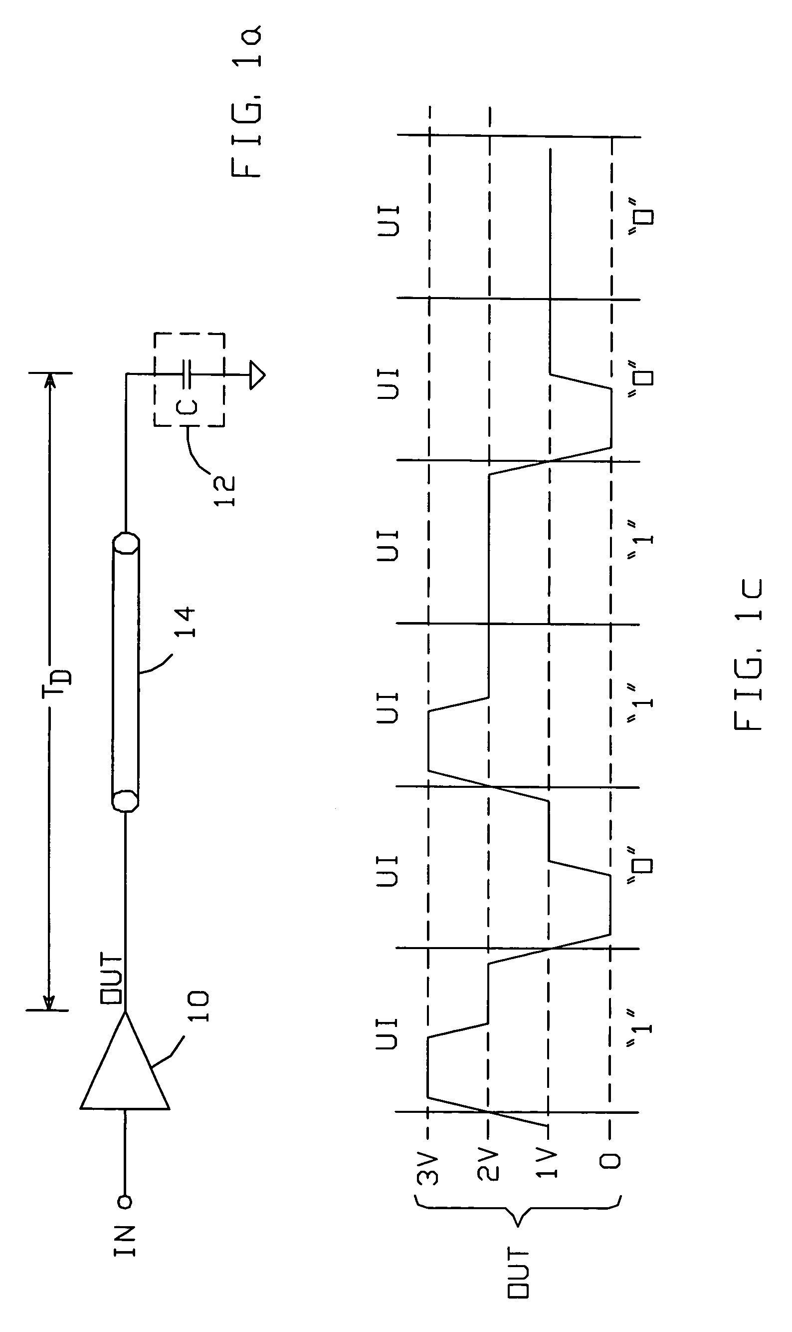
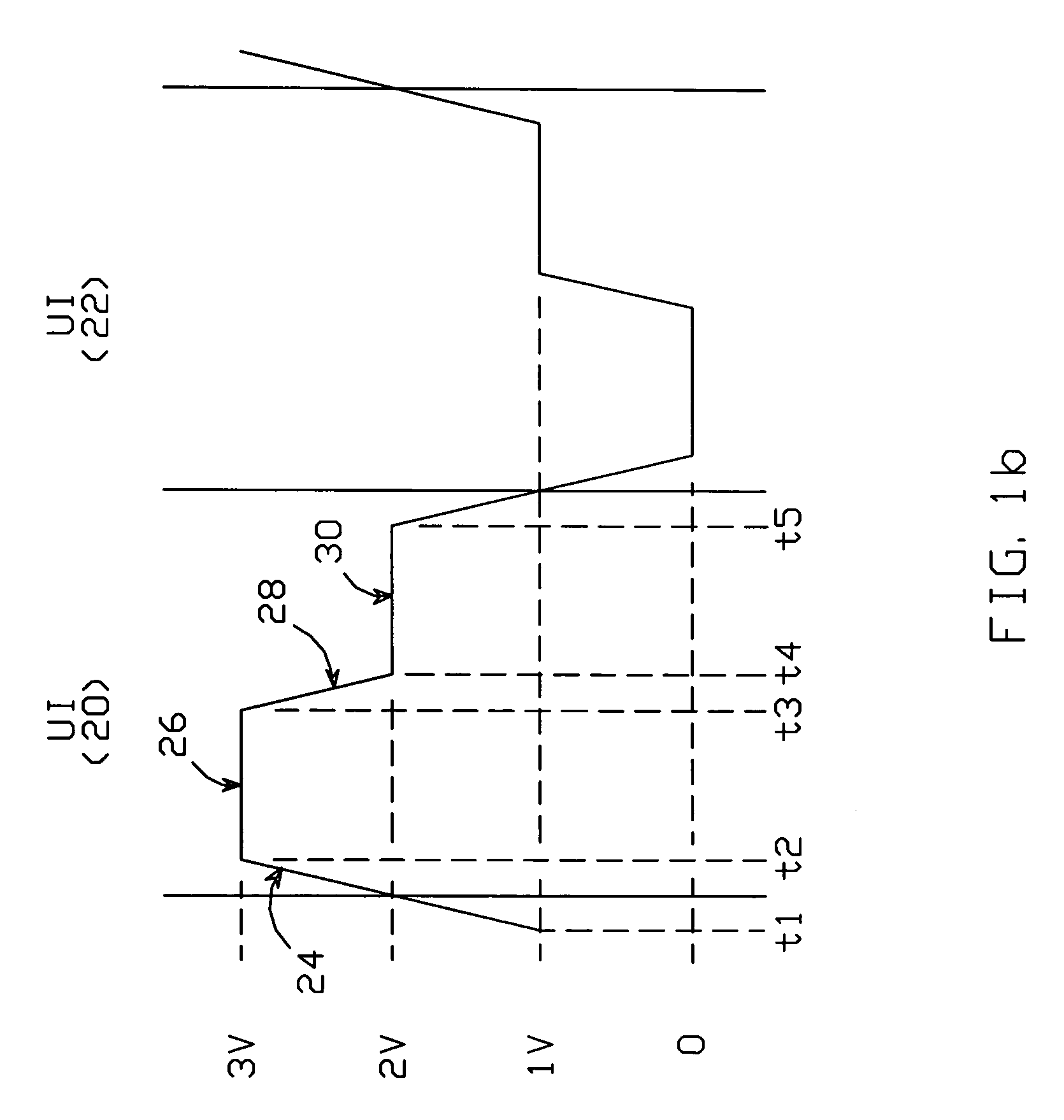
[0025]The present output buffer is intended for driving a capacitively-terminated transmission line as illustrated in FIG. 1a. An output buffer 10 generates a high speed data signal at an output OUT in response to an input signal received at an input terminal IN; the data signal is conveyed to a load 12 via a transmission line 14. Load 12 can be any manner of circuit; for example, a memory cell's address circuitry. The load driven by the data signal includes a capacitive component, such that transmission line 14 is said to be “capacitively-terminated”; in FIG. 1a, the capacitive component of the load is represented as a capacitor C.

[0026]As noted above, a capacitively-terminated transmission line suffers from several problems, including data signal distortion that arises due to data signal transitions which are reflected by load 12 towards source 10, and back again towards the load. Also, an output buffer 10 having a low output impedance provides fast data signal transitions at the ...


PUM


Abstract

An output buffer for driving a capacitively-terminated transmission line produces a waveform which comprises a first portion during which the waveform transitions from a voltage V1 to a voltage V2; a second portion during which it remains fixed at V2; a third portion during which it transitions to a voltage V3; and a fourth portion during which it remains fixed at V3. The waveform is created within a unit interval whenever successive data bits transition between logic states. The first and second portions are generated with circuitry arranged such that V2 is maximized by reducing the buffer's output impedance. The fourth portion is generated with circuitry which has a non-zero output impedance preferably equal to the transmission line's characteristic impedance, to absorb transitions reflected back to the source circuitry by the capacitive termination.

Description

BACKGROUND OF THE INVENTION[0001]1. Field of the Invention[0002]This invention relates to the field of transmission line drivers, and particularly to circuits and methods for driving capacitively-terminated transmission lines.[0003]2. Description of the Related Art[0004]Transmission lines are used to convey high frequency digital data signals between a source circuit and a destination circuit. The destination circuit can be considered a load, which typically includes a capacitive component. Transmission lines having a capacitive load at their receiving end are referred to herein as capacitively-terminated transmission lines.[0005]A transmission line has a characteristic impedance Z0, as does the load being driven. Ideally, the impedances of the load and the transmission line are equal; when so arranged, a data signal transition that occurs at the source end of the transmission line is fully absorbed by the load, with none of the energy reflected back towards the source by the load. ...

Claims


Application Information

Patent Timeline
Patent Type & Authority Patents(United States)
IPC IPC(8): H03K3/00H03K19/003H03K19/0175H04L25/02
CPCH03K19/017545H04L25/026H04L25/0288
Inventor SRIVASTAVA, NIKHIL K.RAGHAVAN, GOPALPOBANZ, CARL W.
Owner MARVELL ASIA PTE LTD
Why Eureka
Try Eureka