Large-sized substrate and method of producing the same

a technology of large-scale substrates and substrates, applied in the field of large-scale substrates, can solve the problems of poor resolution, processing methods, and stuttering of focus positions on the exposure surface, and achieve the effects of high-precision exposure, enhanced register accuracy and resolution, and high-precision exposur

Active Publication Date: 2007-03-20
SHIN ETSU CHEM IND CO LTD
View PDF18 Cites 2 Cited by
  • Summary
  • Abstract
  • Description
  • Claims
  • Application Information

AI Technical Summary

Benefits of technology

[0021]By using the large-sized substrate according to the present invention for light exposure, the exposure accuracy, particularly, the register accuracy and resolution are enhanced, so that it is possible to achieve high-precision exposure for a large-sized panel. In addition, by the processing method according to the present invention, it is possible to stably obtain a large-sized photomask substrate with a high flatness. Since the CD accuracy (dimensional accuracy) at the time of exposure of the panel is enhanced, it is possible to perform exposure of a fine pattern, leading to a higher yield of the panel. Furthermore, by the production method according to the present invention, the step of putting the parallelness into order and the step of putting the flatness into order can be combined into one step, so that the total time required for production is shortened, whereby a large-sized substrate with high accuracy can be obtained economically. Besides, by applying the processing method according to the present invention, it is also possible to create an arbitrary surface shape.

Problems solved by technology

In addition, in the case of an exposure machine which uses an optical system having a focus, there is the phenomenon that the focus position is staggered from the exposure surface with the result of poor resolution.
However, these processing methods have had the following drawback.
In this case, the work is pressed against the work mount table due to the grinding resistance of the processing tool; therefore, if the flatness of the back side of the work is not secured, the flatness of the face side of the work processed conforms to the flatness of the back side, so that the flatness cannot be improved.
Accordingly, in the case of a large-sized photomask substrate, it is very difficult to obtain a high flatness, although it is easy to suppress the dispersion of thickness of the substrate.
However, as the flatness is improved, the elastic deformation amount becomes smaller and, hence, the repelling force also becomes smaller, so that the flatness would not easily be further enhanced.
In such a case, in practice, only the processing margin is increased, and it has been impossible to obtain a substrate with high flatness by the conventional lapping.
This problem is present also in the case of plain surface grinding.

Method used


Image

  • Large-sized substrate and method of producing the same
  • Large-sized substrate and method of producing the same
  • Large-sized substrate and method of producing the same

Examples


example 1

[0047]A synthetic quartz substrate 330×450 mm (diagonal length: 558 mm) in size and 5.3 mm in thickness was processed on a double side lapping device performing a planetary motion by use of GC#600 produced by Fujimi Kenmazai Kogyo. Co. Ltd. to prepare a raw substrate. The accuracy of the raw substrate at this time was a parallelness of 3 μm and a flatness of 22 μm (flatness / diagonal: 3.9×10⁻⁶), and the shape of the raw material was such that a central portion was higher.

[0048]The parallelness and the flatness were measured by use of a flatness tester (FTT-1500) produced by Kuroda Seiko Co., Ltd.

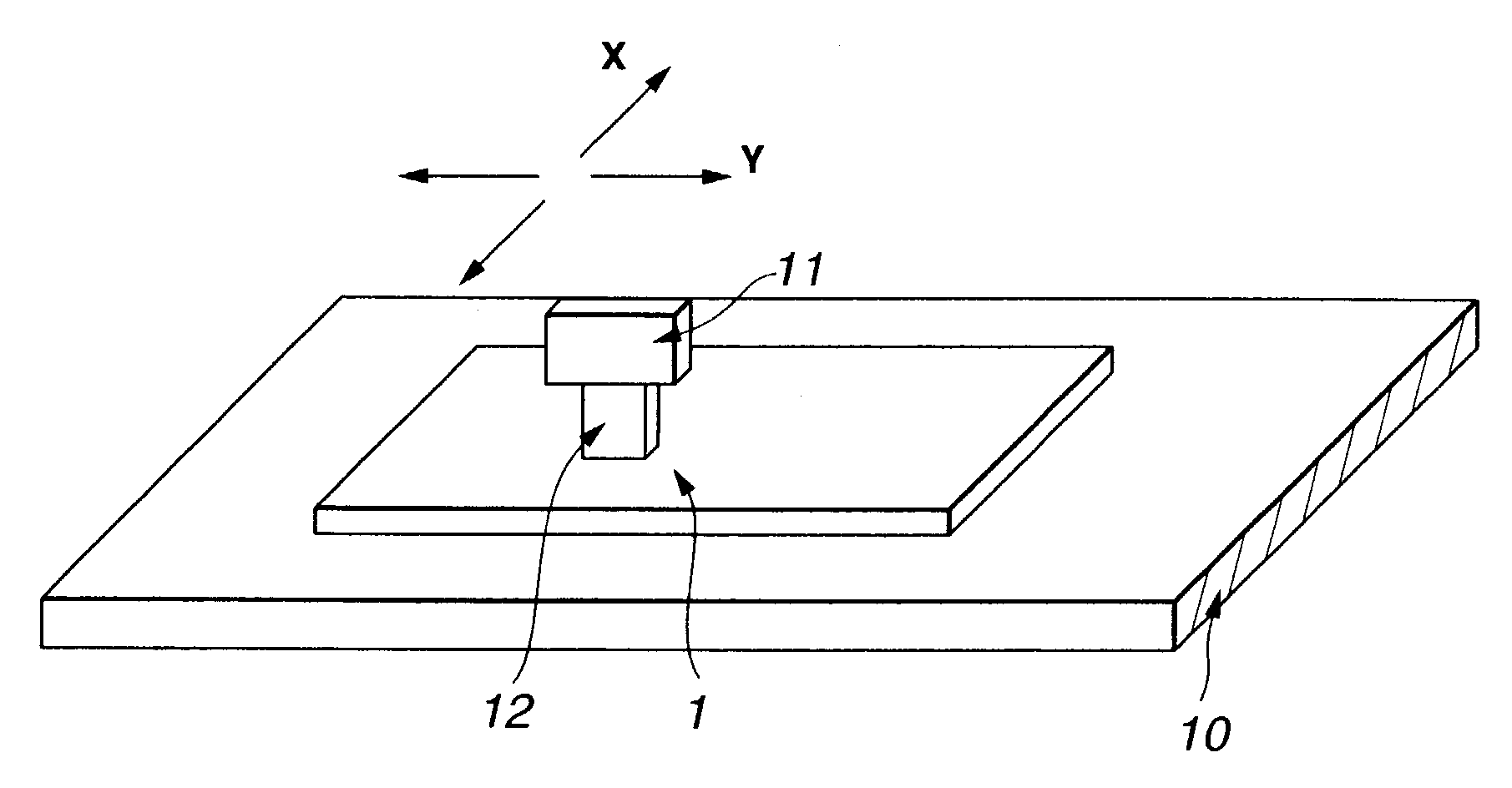
[0049]Then, the plate was mounted on a substrate holding base of the device shown in FIG. 3. In this case, the device used had a structure in which a processing tool is fitted to and rotatable by a motor and a pressure can be applied to the processing tool by air. In addition, the processing tool can be moved substantially in parallel relative to the substrate holding base, in X-axis and Y-ax...

example 2

[0055]Before the same synthetic quartz substrate as that in Example 1 was subjected to 50 μm polish on a double side polishing machine, the substrate was processed by a tool obtained by adhering a cerium pad to a processing tool having an outside diameter of 80 mm and an inside diameter of 50 mm, while pouring a slurry including cerium oxide suspended in water at a concentration of 10 wt % by weight. The processing speed under these conditions was 2 μm / min. The tool movement conditions were determined in the same manner as the moving conditions for the diamond grindstone tool. The processing time was 120 min (total: 220 min). Thereafter, the substrate was subjected to 50 μm polish, and then the flatness was measured to be 1.9 μm (flatness / diagonal: 3.4×10⁻⁶).

example 3

[0056]The process of Example 1 was repeated, except that the processing tool for grinding was not used and only a cerium pad was used as the processing tool.


PUM

PropertyMeasurementUnit
thicknessaaaaaaaaaa
thicknessaaaaaaaaaa
flatness/diagonal lengthaaaaaaaaaa

Abstract

A large-sized substrate having a diagonal length of not less than 500 mm and a ratio of flatness/diagonal length of not more than 6.0×10⁻⁶ is disclosed. By use of the large-sized substrate for exposure of the present invention, the exposure accuracy, particularly the register accuracy and resolution are enhanced, so that it is possible to achieve high-precision exposure of a large-sized panel. With the processing method according to the present invention, it is possible to stably obtain a large-sized photomask substrate with a high flatness, and since the CD accuracy (dimensional accuracy) at the time of exposure of the panel is enhanced, it is possible to perform exposure of a fine pattern, leading to a higher yield of the panel. Furthermore, by applying the processing method according to the present invention, it is also possible to create an arbitrary surface shape.

Description

BACKGROUND OF THE INVENTION[0001]The present invention relates to a large-sized substrate suitable for a synthetic quartz glass substrate for photomask, particularly a substrate for use in a TFT liquid crystal panel, and a method of producing the same.[0002]Generally, for a TFT liquid crystal panel, an active method is adopted in which a liquid crystal is sealed between an array-side substrate with TFT devices incorporated therein and a substrate fitted with a color filter, and voltage is controlled by the TFT to thereby control the orientation of the liquid crystal.[0003]At the time of producing the array side, a method is adopted in which images are printed on a mother glass such as non-alkali mother glass in a multiple layers by light exposure through originals carrying circuits drawn thereon, called large-sized photomasks. On the other hand, the color filter side is also produced by a method using lithography, called a dye impregnation method. The large-sized photomasks are requ...

Claims


Application Information

Patent Timeline
Patent Type & Authority Patents(United States)
IPC IPC(8): B32B17/00G03F9/00B24B7/00B24C1/00C03C19/00G02F1/1333G03F1/00G03F1/60G03F1/68
CPCB24B7/00B24C1/00C03C19/00G03F1/14G03F1/60Y10T428/315G02F2001/133302G02F1/133302G03F1/00G03F1/68
Inventor SHIBANO, YUKIOMIHARADA, SATORUUEDA, SHUHEIWATABE, ATSUSHITABATA, MASAKI
Owner SHIN ETSU CHEM IND CO LTD
Why Eureka
Try Eureka