Drive methods and drive devices for active type light emitting display panel

a technology of light-emitting display panel and drive device, which is applied in the direction of static indicating device, electroluminescent light source, instruments, etc., can solve the problems of time rate, long time, and substantially high impedance of the device,

Inactive Publication Date: 2007-03-20
TOHOKU PIONEER CORP
View PDF6 Cites 187 Cited by
  • Summary
  • Abstract
  • Description
  • Claims
  • Application Information

AI Technical Summary

Problems solved by technology

Furthermore, since the constant current drive is performed as described above, its impedance is substantially high, and therefore rising to the light emission threshold voltage of the EL element necessitates a longer time.
Thus, a lighting time rate of an EL element decreases, thereby resulting in a substantially deteriorated light-emitting efficiency.
Problems that respective EL elements are affected by variations in times that are until EL elements are brought to the light emitting state and the like and therefore linearity of gradation control is deteriorated and the like occur.

Method used


Image

  • Drive methods and drive devices for active type light emitting display panel
  • Drive methods and drive devices for active type light emitting display panel
  • Drive methods and drive devices for active type light emitting display panel

Examples


first embodiment

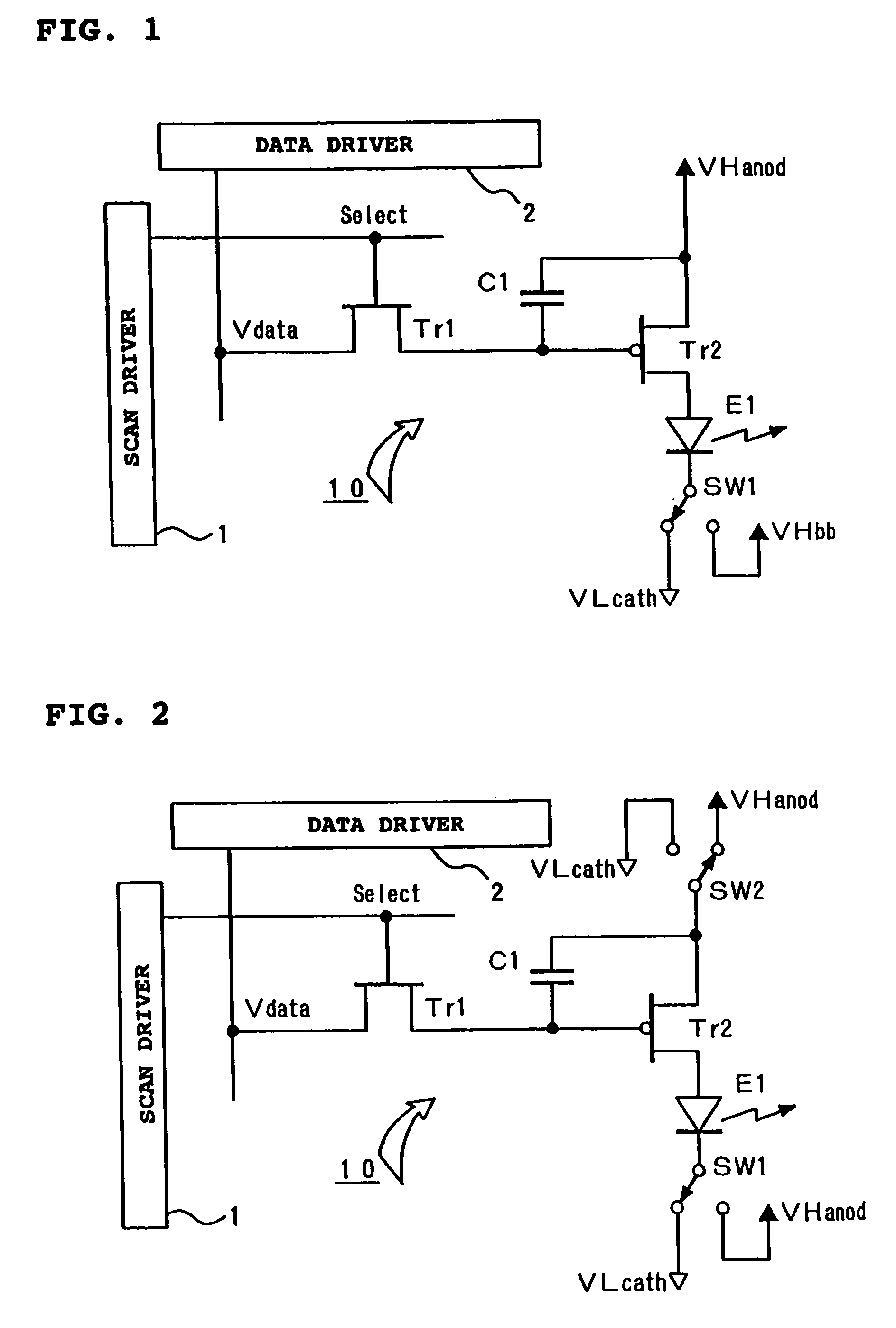
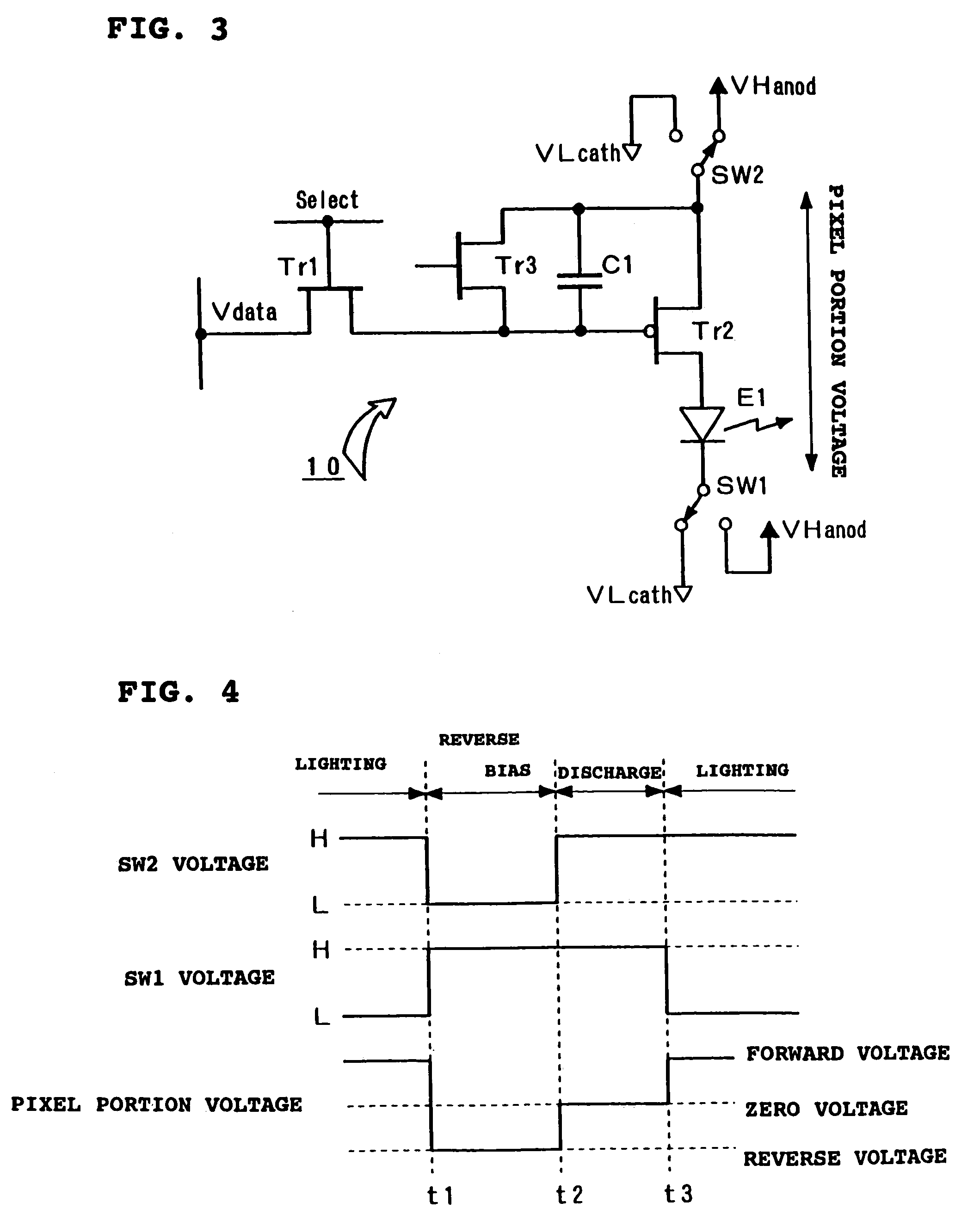
[0048]The first form of a drive device according to the present invention not only can be applied to one in which a drive means by the conductance control technique is utilized as shown in FIG. 2 but also can be suitably utilized in a light emitting display panel provided with a three TFT technique pixel 10 which realizes digital gradation for example shown in FIG. 3. Further, the first embodiment in the first form of a drive device according to the present invention can be applied similarly to a light emitting display panel provided with a pixel by voltage programming technique, threshold voltage correction technique, or current mirror technique which will be explained later.

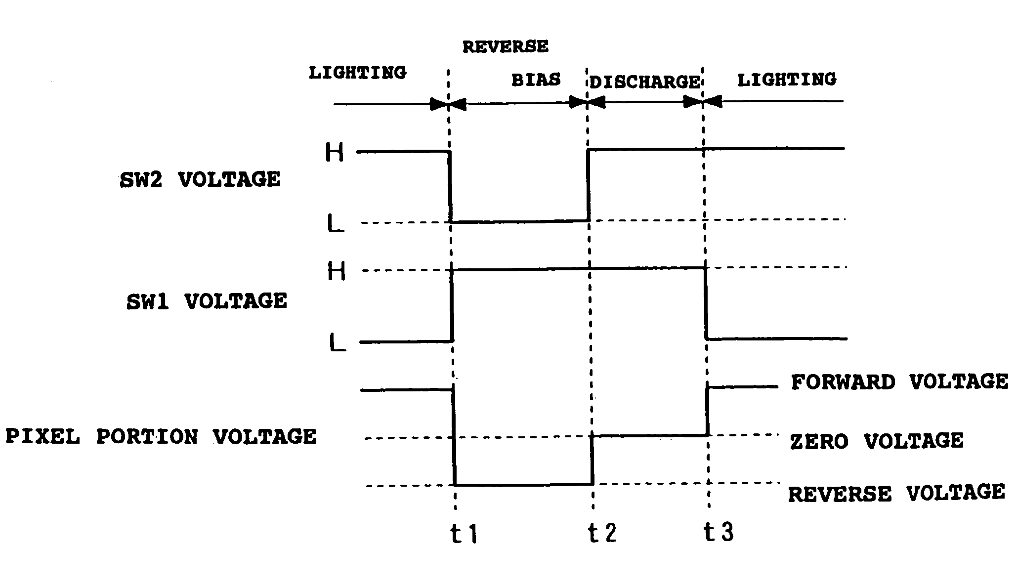
[0049]In the structure provided with a pixel 10 of the three TFT technique shown in FIG. 3, an erasing TFT (Tr3) is provided for the structure shown in FIG. 2, and by allowing this erasing TFT (Tr3) to perform an ON operation in the middle of a lighting period of the EL element E1, electrical charges of the cap...

second embodiment

[0057]Next, FIG. 5 explains the first form of a drive device according to the present invention. This FIG. 5 shows the basic structure comprised of the driving TFT (Tr2), the EL element E1, and the capacitor C1, and other portions are omitted. In the structure shown in this FIG. 5 also, the above-described conductance control technique or a pixel structure of the three TFT technique which realizes digital gradation can be adopted, and further the structure can be similarly applied to a light emitting display panel provided with a pixel by the voltage programming technique, threshold voltage correction technique, or current mirror technique which will be explained later.

[0058]In the second embodiment of the first form shown in FIG. 5, a switch SW1 arranged in a cathode side of the EL element E1 constitutes a three input select switch. A switch SW3 is connected between the anode and the cathode of the EL element E1. By switching the switch SW3 on, the anode and the cathode of the EL e...

third embodiment

[0090]FIG. 13 shows the fourth form according to the present invention, and the structure shown in this FIG. 13 is called the threshold voltage correction technique herein. In this threshold voltage correction technique shown in FIG. 13, the EL element E1 is connected in series to the driving TFT (Tr2), and the capacitor C1 for holding electrical charges is connected between the gate and the source of the driving TFT (Tr2). That is, this basic structure is similar to that shown in FIG. 1.

[0091]In the structure shown in FIG. 13, a parallel connection part of a TFT (Tr4) and a diode D1 is inserted between a switch SW9 (this is equivalent to the controlling TFT (Tr1)) connected to the data line and the gate of the driving TFT (Tr2). The TFT (Tr4) is constructed so that its gate and-drain are in a short circuit state, and therefore this TFT functions as an element which imparts a threshold characteristic from the switch SW9 toward the gate of the driving TFT (Tr2).

[0092]With this struct...


PUM


Abstract

In a drive device for an active type light emitting display panel which can apply a reverse bias voltage to an EL element, in order to be able to compensate deterioration in light-emitting efficiency of the EL element accompanied by applying of the reverse bias voltage and the like, one pixel 10 is composed of a controlling TFT (Tr1), the driving TFT (Tr2), a capacitor C1, and the EL element E1. Switching switches SW1, SW2 mutually enables a supplying state of a forward current to the EL element E1 and an applying state of the reverse bias voltage to be selected. In one control form according to the present invention, when the applying state of the reverse bias voltage shifts to the supplying state of the forward current, by switching one switch first, the anode and cathode of the EL element E1 are made to the same electrical potential to allow electrical charges to be discharged. Thus, charge of the forward current for a parasitic capacitance of the EL element E1 can be performed rapidly, and rising of the lighting operation of the EL element can be advanced.

Description

BACKGROUND OF THE INVENTION[0001]1. Field of the Invention[0002]The present invention relates to drive devices for a light emitting display panel in which a light emitting element constituting a pixel is actively driven by a TFT (thin film transistor) and in which a reverse bias voltage can be applied to the light emitting element, and particularly to drive methods and drive devices for an active type light emitting display panel in which deterioration in light-emitting efficiency of the light emitting element accompanied by applying of the reverse bias voltage and the like can be compensated.[0003]2. Description of the Related Art[0004]A display using a display panel which is constructed by arranging light emitting elements in a matrix pattern has been developed widely. As the light emitting element employed in such a display panel, an organic EL (electro-luminescent) element in which an organic material is employed in a light emitting layer has attracted attention. This is because...

Claims


Application Information

Patent Timeline
Patent Type & Authority Patents(United States)
IPC IPC(8): G09G3/30H01L51/50G09G3/10G09G3/20G09G3/32H05B33/14
CPCG09G3/3233G09G3/3241G09G3/325G09G2300/0809G09G2300/0819G09G2320/043G09G2300/0852G09G2300/0866G09G2310/0254G09G2310/0256G09G2320/0252G09G2300/0842G09G3/30
Inventor YOSHIDA, TAKAYOSHIKANAUCHI, KATSUHIRO
Owner TOHOKU PIONEER CORP
Why Eureka
Try Eureka