Memory interlace-checking method

a memory interlace and interlace technology, applied in the field of memory interlace-checking method, can solve the problems of low stability, inability to accurately detect memory weakening or instability, and one bit by one bit access method cannot effectively detect memory weakening problems, etc., and achieve the effect of accurate detection

Inactive Publication Date: 2007-03-27
WINBOND ELECTRONICS CORP
View PDF3 Cites 0 Cited by
  • Summary
  • Abstract
  • Description
  • Claims
  • Application Information

AI Technical Summary

Benefits of technology

[0011]The memory interlace-checking method in accordance with the present invention includes: a main step having at least a main datum, which performs command actions on the memory address row or column; a data checking step having at least a data check datum, which checks memory rows or columns not triggered in the main step; wherein by accessing particular memory rows or columns, other yet to be triggered memory rows or columns may be weakened by electromagnetic interference (EMI) and thus can be accurately detected in the data checking step.

Problems solved by technology

Under such a high density, a low operation voltage and a high operation frequency, memory becomes very sensitive and is easily damaged or weakened because of the manufacturing process, external signals or noise generated inside, resulting in low stability.
According to the current state of the art in memory testing, there is a problem of being unable to accurately detect memory weakening or instability.
This kind of one bit by one bit access method cannot effectively detect memory weakening problems.
That is, as shown in FIG. 6A, when accessing the first row from left to right, electromagnetic interference (EMI) may result in weakening in the next row.
Therefore, the foregoing continuous memory address accessing scheme cannot effectively detect the memory weakening problems.
The conventional memory test methods are neither stringent nor accurate and thus have to be improved.

Method used


Image

  • Memory interlace-checking method
  • Memory interlace-checking method
  • Memory interlace-checking method

Examples


Embodiment Construction

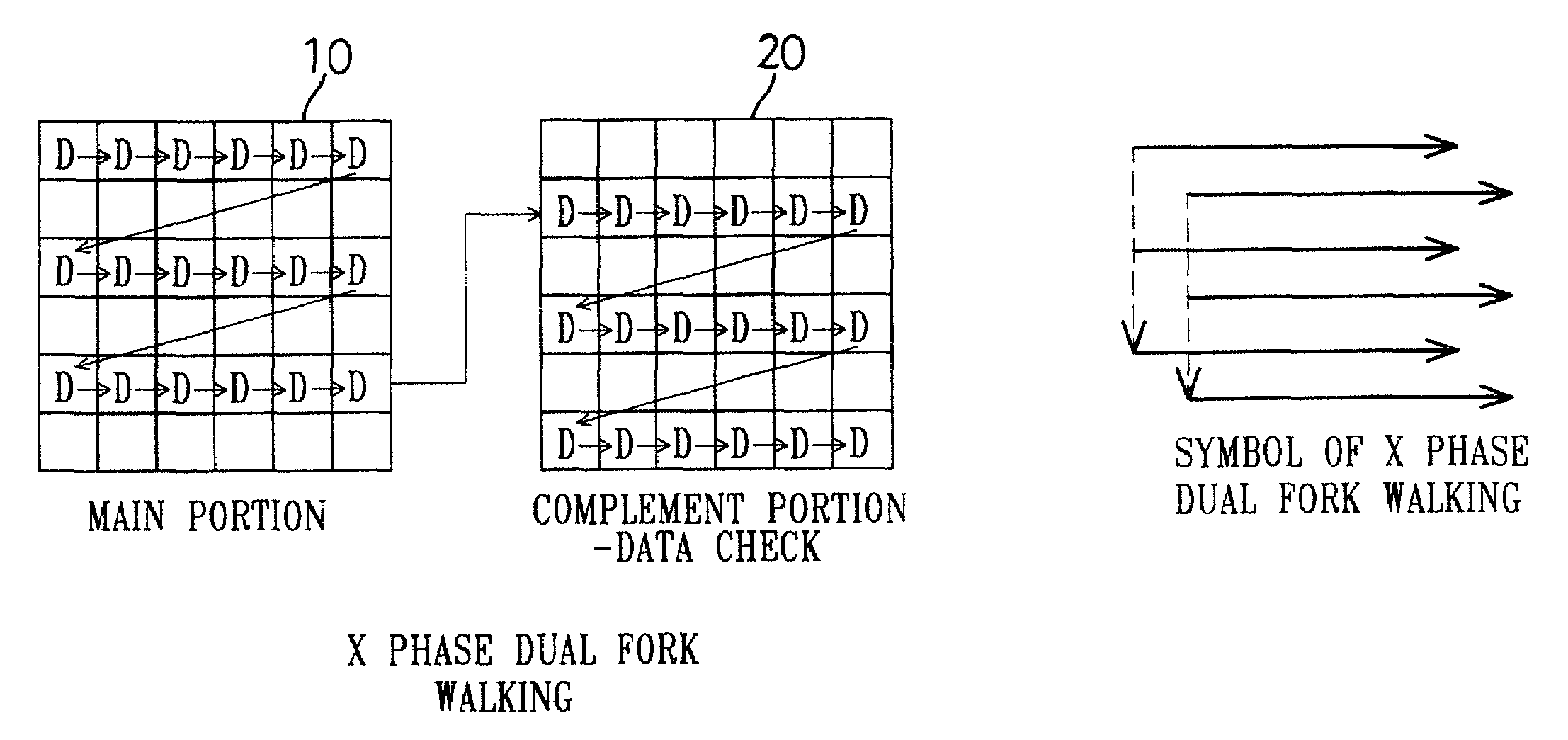
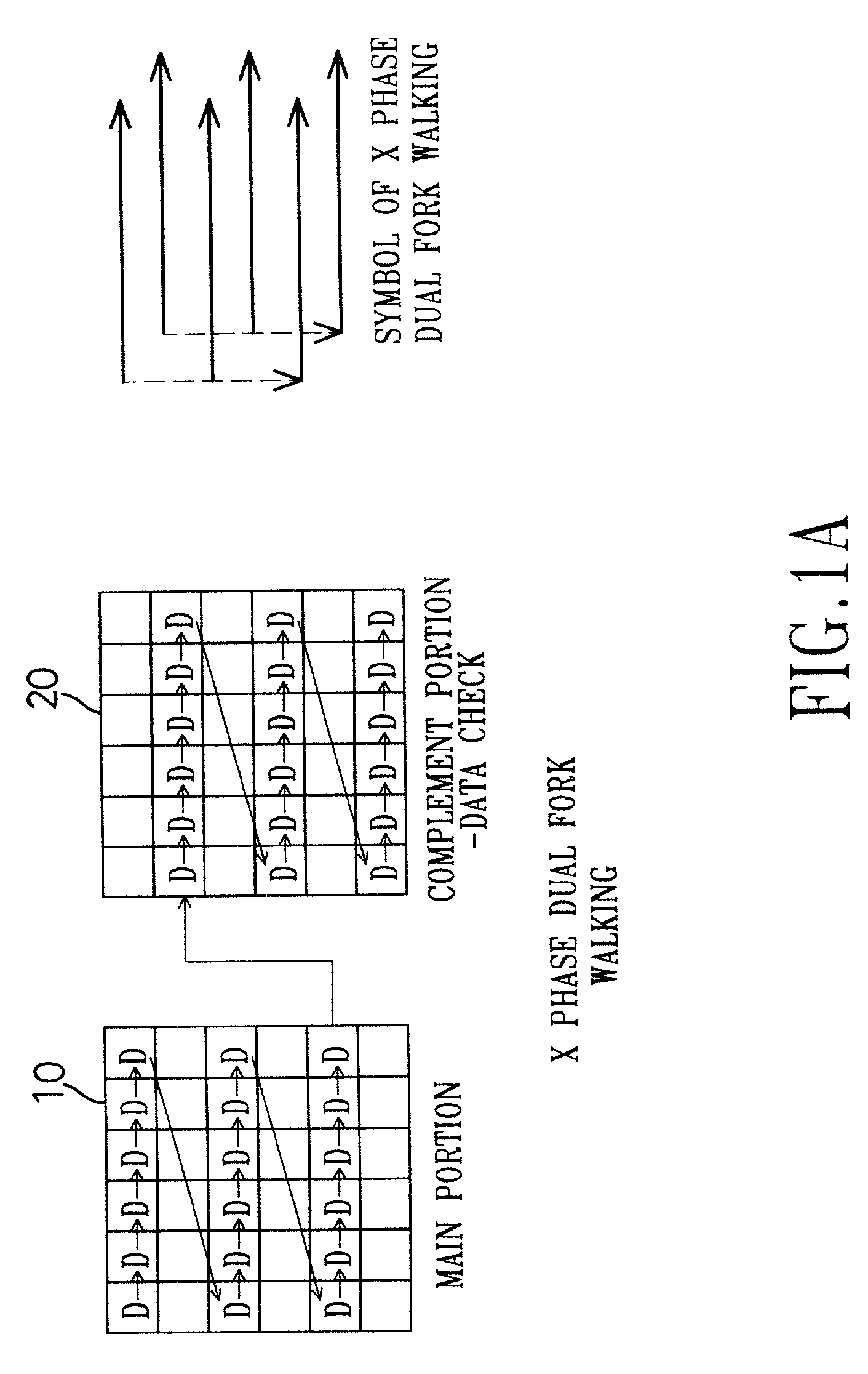
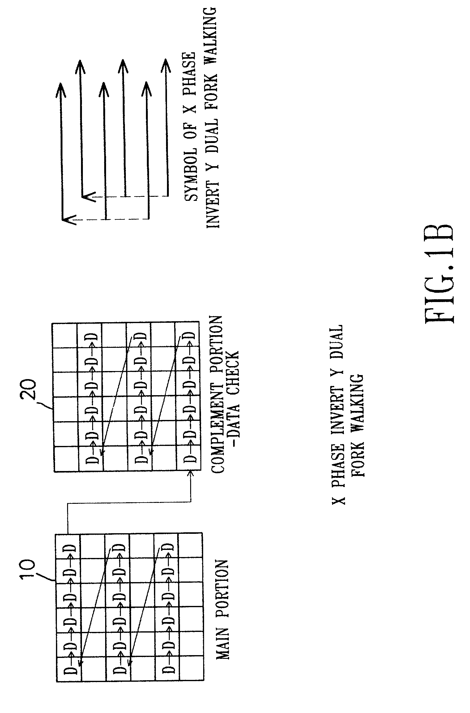
[0018]The test method in accordance with the present invention can more accurately detect memory weakening problems. This method is different from conventional address accessing continuous sequential address accessing. The present invention uses an interlacing data access technique. The method in accordance with the present invention is composed of at least two steps: the main step and the data checking step. In the main step, there are main data for executing commands. The data perform the write, read, or refresh command in local addresses in the memory (such as from left to right or from right to left in odd or even columns or rows). While accessing the odd columns (rows), the yet to be accessed memory addresses, i.e., the even columns (rows), are weakened by the electromagnetic interference (EMI) induced from the previously mentioned command actions. Afterwards, the data checking step provides checking commands that checks addresses yet to be triggered in the main step, i.e., the...


PUM


Abstract

The present invention relates to a memory interlace-checking method and, in particular, to a test method that can effectively detect the weakening of memory. This test method is different from the conventional continuous address testing style. It is an interlacing address test method that comprises a main step and a data checking step. The main step provides main data to perform command actions on local addresses in memory. This will weaken other portions in the memory that are not trigged by commands because of the electromagnetic interference (EMI) induced by memory operations. Afterwards, in the data checking step, the yet to be triggered portion will be checked in a complementary way in order to accurately detect weakened memory.

Description

BACKGROUND OF THE INVENTION[0001]1. Field of Invention[0002]The present invention relates to a memory interlace-checking method, which is a test method that can detect weakened memory. Through interlacing data accesses, the method can more accurately find memory problems.[0003]2. Related Art[0004]Memory is an indispensable element in a computer system. It has a deterministic influence on the stability of the system. As the capacity and speed of the memory increase indefinitely, the current memory manufacturing technologies reach a scale below 0.2 micrometers, a supply voltage below 3.3 volts, and an operation speed over 133 MHz. Under such a high density, a low operation voltage and a high operation frequency, memory becomes very sensitive and is easily damaged or weakened because of the manufacturing process, external signals or noise generated inside, resulting in low stability. Therefore, how to accurately quickly detect the memory weakening problem is an important subject studie...

Claims


Application Information

Patent Timeline
Patent Type & Authority Patents(United States)
IPC IPC(8): G11C29/00G11C29/02
CPCG11C29/02
Inventor LEE, CHEN-TSAI
Owner WINBOND ELECTRONICS CORP
Why Eureka
Try Eureka