Flash memory device with improved erase function and method for controlling erase operation of the same

a flash memory and erase function technology, applied in the field of flash memory devices and control of erase operations, can solve problems such as failure in read operations, shallow erase, and disturbance of erase, and achieve the effects of reducing the number of failed read operations, and increasing the depth of erase operations

Active Publication Date: 2007-04-03
SK HYNIX INC
View PDF4 Cites 21 Cited by
  • Summary
  • Abstract
  • Description
  • Claims
  • Application Information

AI Technical Summary

Benefits of technology

[0009]Accordingly, the present patent addresses the above problems, and discloses flash memory devices in which a shallow erase phenomenon of non-selected memory cell blocks due to the leakage current of pass gates can be prevented by applying a positive bias voltage to a global word line in an erase operation.
[0010]The present patent also discloses a method of controlling an erase operation of flash memory devices, wherein a shallow erase phenomenon of non-selected memory cell blocks due to the leakage current of pass gates can be prevented by applying a positive bias voltage to a global word line in an erase operation.

Problems solved by technology

Therefore, there is a problem in that a phenomenon (i.e., a shallow erase) in which a small amount of electrons is discharged from floating gates of memory cells CB1 to CBn that should not be erased.
Erase disturbance, such as shallow erase, becomes more profound when the number of memory cell blocks included in a flash memory device increases.
Consequently, as the threshold voltages of corresponding memory cells gradually decrease, there is a problem in that fail occurs in the read operation.

Method used


Image

  • Flash memory device with improved erase function and method for controlling erase operation of the same
  • Flash memory device with improved erase function and method for controlling erase operation of the same
  • Flash memory device with improved erase function and method for controlling erase operation of the same

Examples


Embodiment Construction

[0024]Now, the various embodiments according to the present patent will be described with reference to the accompanying drawings. Because various embodiments are provided for the purpose that the ordinary persons skilled in the art are able to understand the present patent, they may be modified in various manners and the scope of the present patent is not limited by the various embodiments described later.

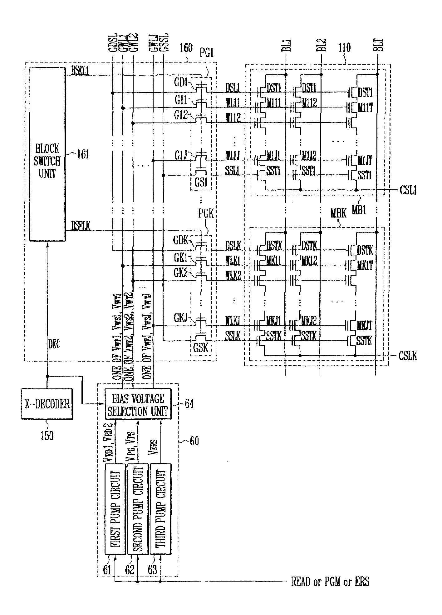
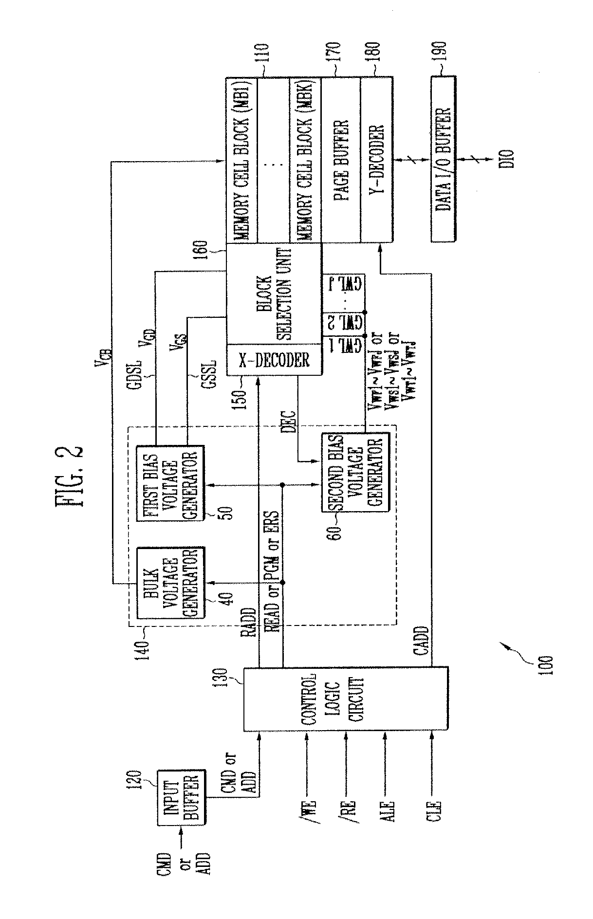
[0025]FIG. 2 is a block diagram of a flash memory device according to an embodiment of the present patent.

[0026]Referring to FIG. 2, a flash memory device 100 includes a memory cell array 110, an input buffer 120, a control logic circuit 130, a high voltage generator 140, a X-decoder 150, a block selection unit 160, a page buffer 170, a Y-decoder 180 and a data I / O buffer 190. The memory cell array 110 includes memory cell blocks MB1 to MBK (where K is an integer), each having a plurality of memory cells (not shown). The input buffer 120 receives a command signal CMD or an address ...


PUM


Abstract

The present patent relates to flash memory devices with improved erase function, and method of controlling an erase operation of the same. According to the present patent, the flash memory device includes memory cell blocks, each having a plurality of memory cells sharing local word lines and bit lines, an X-decoder which decodes a row address signal and outputs the decoded signal, a block selection unit, which selects some of the memory cell blocks in response to the decoded signal, and connects local word lines of the selected memory cell blocks to corresponding global word lines, respectively, and a high voltage generator, which generates word line bias voltages in response to one of a read command, a program command and an erase command, and supplies the generated word line bias voltages to the global word lines in response to the decoded signal, respectively, wherein the word line bias voltages, which are generated by the high voltage generator in response to the erase command, have a positive value, respectively. Accordingly, a positive bias voltage is applied to a global word line in an erase operation. It is thus possible to prevent a shallow erase phenomenon of non-selected memory cell blocks due to the leakage current of pass gates.

Description

CROSS REFERENCE TO RELATED APPLICATIONS[0001]This application relies for priority upon Korean Patent Application No. 2005-0020182 filed on Mar. 10, 2005, the contents of which are herein incorporated by reference in their entirety.[0002]1. Field of the Patent[0003]The present patent relates to semiconductor memory devices and method of controlling the operation of the same, and more specifically, to flash memory devices and method of controlling the erase operation of the same.[0004]2. Discussion of Related Art[0005]Generally, flash memory devices can be classified into a NOR type, which is generally used to store a small quantity of information at high speed, and a NAND type, which is generally used to store a great amount of information. Further, the flash memory device performs a read operation, a program operation and an erase operation. More particularly, the program operation and the erase operation of the NAND type flash memory device are executed by means of Fowler-Nordheim ...

Claims


Application Information

Patent Timeline
Patent Type & Authority Patents(United States)
IPC IPC(8): G11C16/04
CPCG11C16/16G11C16/30G11C16/0483G10K9/04G10K9/18
Inventor LEE, HEE
Owner SK HYNIX INC
Why Eureka
Try Eureka