Semiconductor device, display device, and signal transmission system

Inactive Publication Date: 2007-05-08
CYPRESS SEMICONDUCTOR
View PDF6 Cites 0 Cited by
  • Summary
  • Abstract
  • Description
  • Claims
  • Application Information

AI Technical Summary

Benefits of technology

[0052]The present invention is made in view of the above problems, and the object of the present invention is to provide a semiconductor device, a

Problems solved by technology

Therefore, sometimes, the accumulated error of the duty ratio of the signal after the signal passes through the drivers in multiple stages becomes unignorable.
Therefore, there is a possibility that normal shapes of signals cannot be maintained during

Method used


Image

  • Semiconductor device, display device, and signal transmission system
  • Semiconductor device, display device, and signal transmission system
  • Semiconductor device, display device, and signal transmission system

Examples


Example

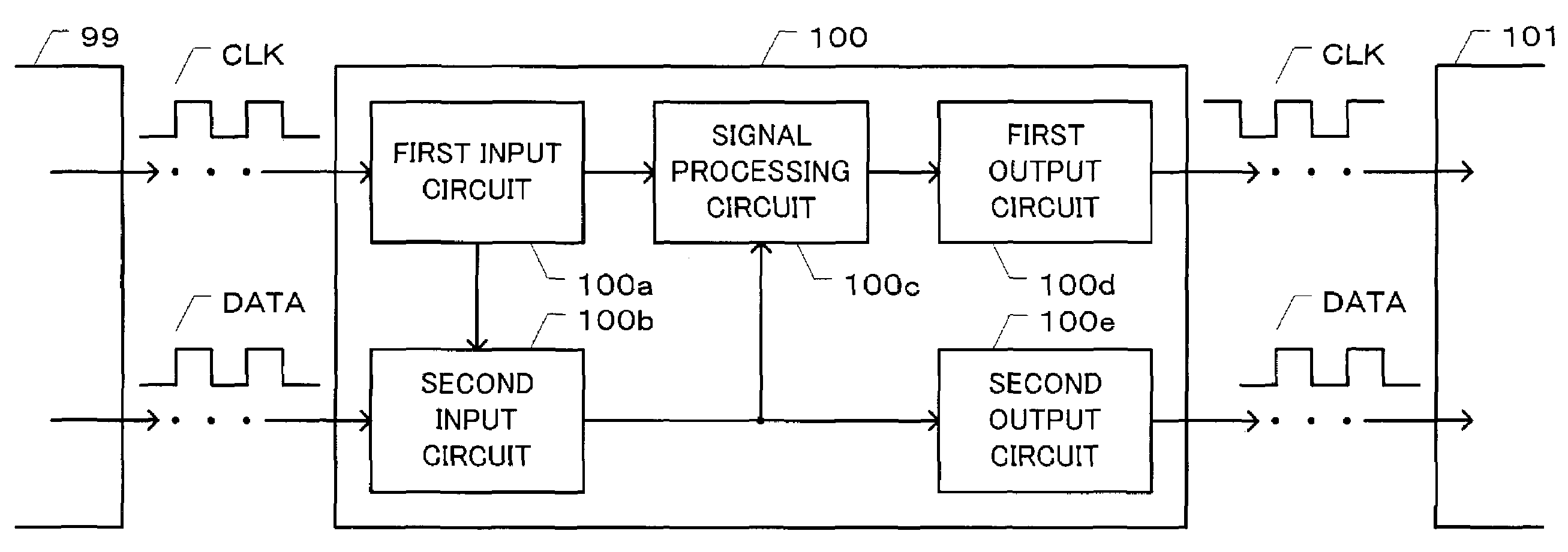
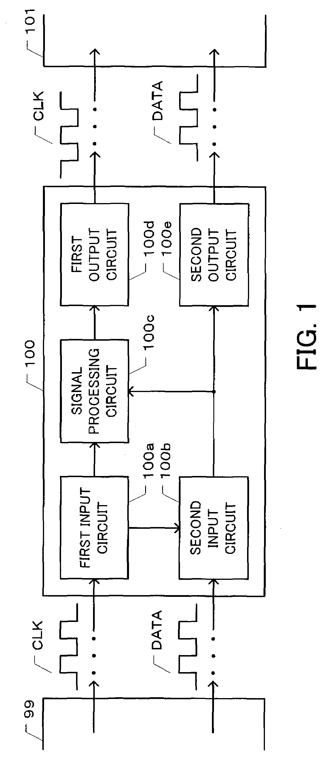
[0077]An embodiment of the present invention is explained below with reference to drawings.

[0078]FIG. 1 is a diagram for explaining the principle of the present invention. As illustrated in FIG. 1, the semiconductor device 100 is cascade-connected between the semiconductor devices 99 and 101. The semiconductor device 100 receives a clock signal (CLK) and a data signal (DATA) which are outputted from the semiconductor device 99 in the preceding stage, performs predetermined signal processing, and outputs a clock signal and a data signal to the semiconductor device 101 in the following stage.

[0079]The semiconductor device 100 comprises a first input circuit 100a, a second input circuit 100b, a signal processing circuit 100c, a first output circuit 100d, and a second output circuit 100e.

[0080]The first input circuit 100a receives a clock signal as a first signal supplied from the semiconductor device 99 in the preceding stage.

[0081]The second input circuit 100b receives a data signal ...


PUM


Abstract

A display device includes a plurality of data drivers which are cascade-connected, and prevents variation of the duty ratio of a signal caused by accumulation of errors. In each of the plurality of data drivers: a first input circuit receives a first signal supplied from outside; a second input circuit receives a second signal supplied from outside, in response to the first signal received by the first input circuit; a signal processing circuit performs signal processing based on the second signal received by the second input circuit; a first output circuit inverts the first signal received by the first input circuit, and outputs the inverted first signal; and a second output circuit delays the second signal received by the second input circuit, by a predetermined amount, and outputs the delayed second signal.

Description

CROSS-REFERENCE TO RELATED APPLICATIONS[0001]This application is based upon and claims the benefits of priority from the prior Japanese Patent Application No. 2002-149929, filed on May 24, 2002, the entire contents of which are incorporated herein by reference.BACKGROUND OF THE INVENTION[0002]1) Field of the Invention[0003]The present invention relates to a semiconductor device, a display device, and a signal transmission system. In particular, the present invention relates to a semiconductor device which is cascade-connected and processes signals, and a display device and a signal transmission system which include a cascade connection and processes signals.[0004]2) Description of the Related Art[0005]For example, in liquid crystal display (LCD) devices, pixels each including a transistor are arranged in rows and columns, gate bus lines extending in the horizontal direction are connected to gates of the transistors in the pixels, and data bus lines extending in the vertical directio...

Claims


Application Information

Patent Timeline
IPC IPC(8): G09G3/36G02F1/133G09G3/20
CPCG09G3/20G09G3/3688G09G2370/08G09G2310/08G09G2310/0275G09G3/36
Inventor KUMAGAI, MASAOUDO, SHINYA
Owner CYPRESS SEMICONDUCTOR
Why Eureka
Try Eureka