Stacked-type semiconductor device

a semiconductor and stacked technology, applied in the direction of solid-state devices, basic electric elements, electrical apparatus construction details, etc., can solve the problems of difficult to effectively reduce the thickness of the device as a whole, and the configuration may not be advantageous in terms of saving production costs, so as to reduce the thickness of the device, reduce the cost, and reduce the defect of the electrode terminal connection portion due to the bending of the wiring substra

Active Publication Date: 2007-05-15
SOCIONEXT INC
View PDF18 Cites 36 Cited by
  • Summary
  • Abstract
  • Description
  • Claims
  • Application Information

AI Technical Summary

Benefits of technology

[0009]In Japanese Laid-open Patent Application No. 2001-223297 mentioned above, there is no specific disclosure concerning an electromagnetic shield prepared for the stacked-type semiconductor device for conforming to the above-mentioned EMI regulation. Further, although there is a disclosure of considering the EMI regulation for the stacked-type semiconductor device in Japanese Laid-open Patent Application No. 2000-174204 also mentioned above, the first substrate has a shape of a cavity as mentioned above, and also, the airtight sealing is provided, whereby such a configuration may not be advantageous in terms of saving the production costs. Furthermore, since this configuration has the metal cover as mentioned above, it may be difficult to effectively reduce the thickness of the device as a whole. Therefore, it is then demanded to provide a stacked-type semiconductor device having a radio-frequency circuit device mounted therein in a mixed loading manner, electromagnetic radiation therefrom being able to be reduced to a lowest possible level, and also, requiring reduced production costs and effectively miniaturized as a whole.
[0011]According to the present invention, by providing such a configuration, it is possible to provide a stacked-type semiconductor device in which a level of electromagnetic radiation generated from a radio-frequency circuit device mounted therein in a mixed loading manner can be well controlled, and also, which can be produced in a reduced thickness (miniaturized) with reduced costs, in comparison to a configuration in the related art. Furthermore, according to the present invention, since the wiring substrates are connected together not only with the electrode terminals which connect these wiring substrates together but also with the conductor supporting member, manufacturing defects in electrode terminal connection portions due to bending of the wiring substrates or such can be effectively reduced, and thus, it is possible to provide a stacked-type semiconductor device improved in the connection reliability between the wiring substrates thereof.

Problems solved by technology

Further, although there is a disclosure of considering the EMI regulation for the stacked-type semiconductor device in Japanese Laid-open Patent Application No. 2000-174204 also mentioned above, the first substrate has a shape of a cavity as mentioned above, and also, the airtight sealing is provided, whereby such a configuration may not be advantageous in terms of saving the production costs.
Furthermore, since this configuration has the metal cover as mentioned above, it may be difficult to effectively reduce the thickness of the device as a whole.

Method used


Image

  • Stacked-type semiconductor device
  • Stacked-type semiconductor device
  • Stacked-type semiconductor device

Examples


first embodiment

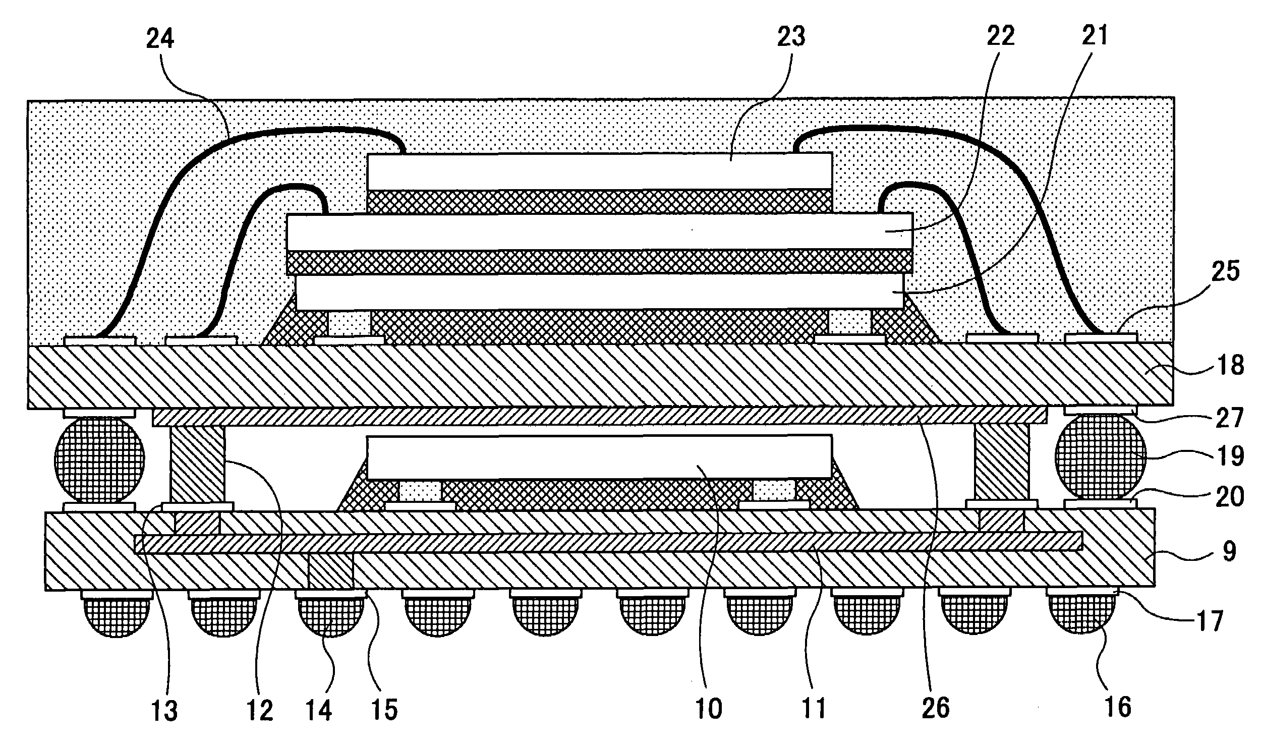
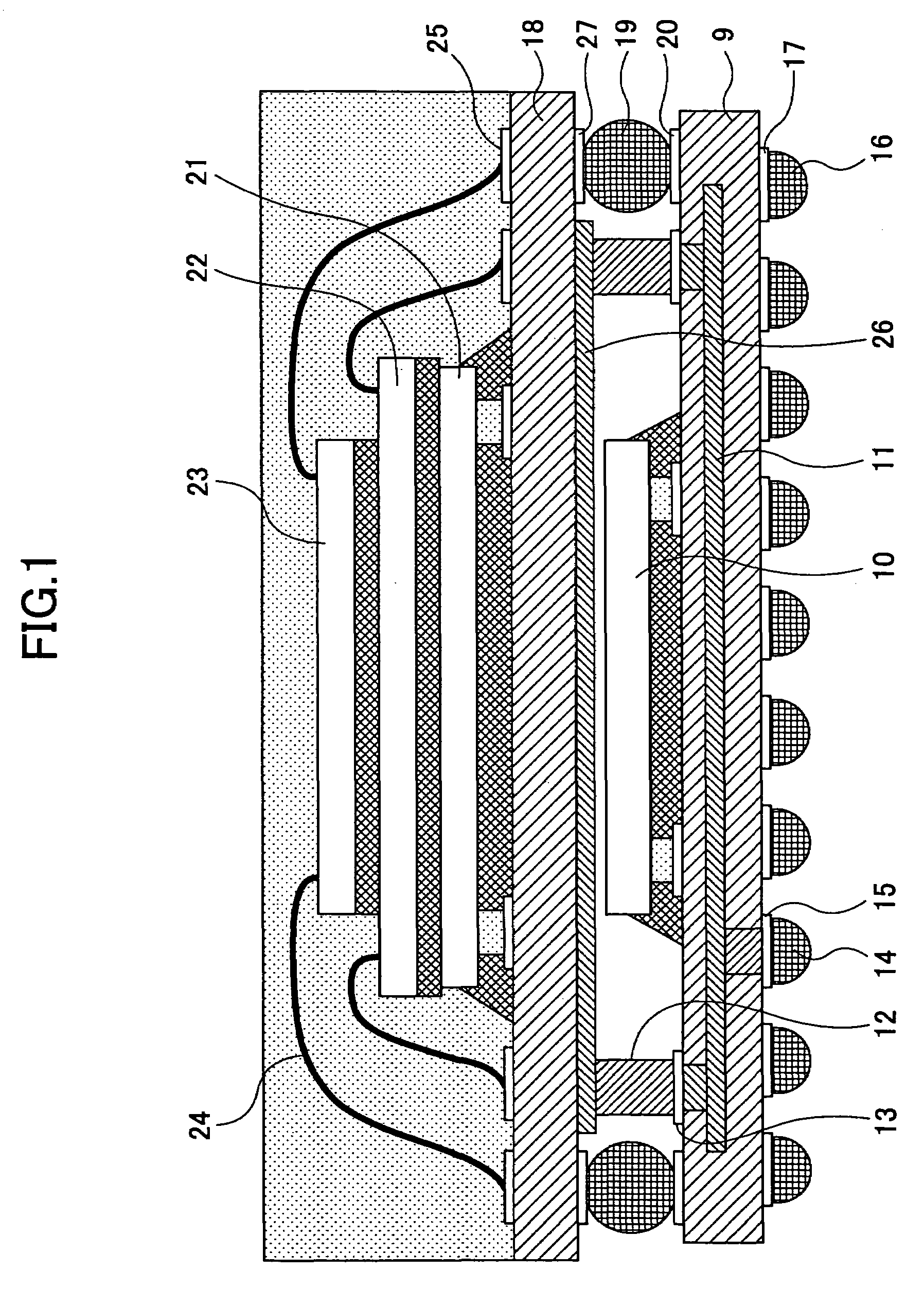
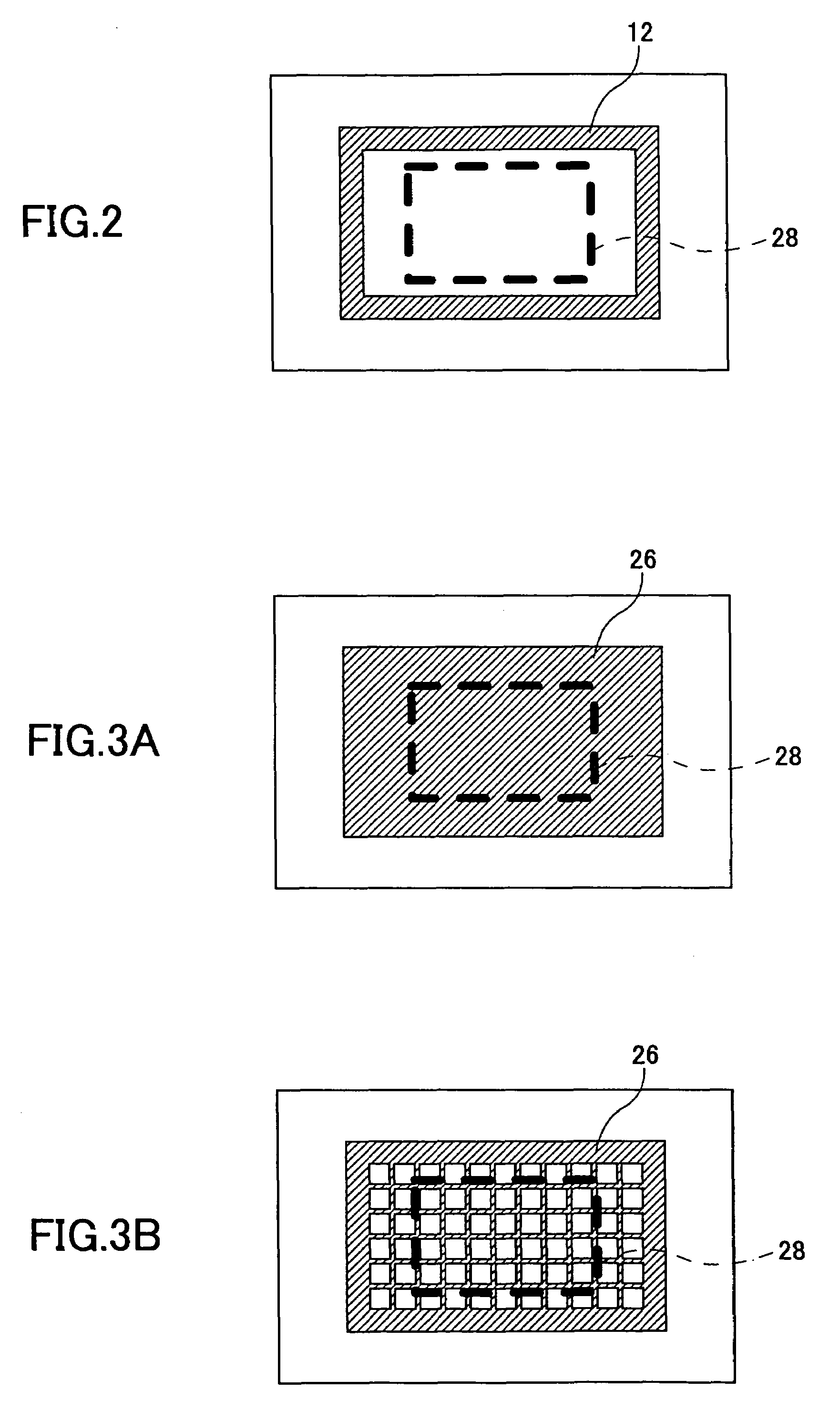
[0022]FIG. 1 shows a side elevational sectional view of a stacked-type semiconductor device in the present invention; FIG. 2 shows a plan view illustrating a structure of a conductor supporting member 12 in the stacked-type semiconductor device shown in FIG. 1; and FIGS. 3A and 3B show plan view respectively illustrating alternative examples of a pattern of a ground wiring layer 26 in the stacked-type semiconductor device shown in FIG. 1. As shown in the figures, the stacked-type semiconductor device includes wiring substrates 9 and 18; ground wiring layers 11 and 26; the conductor supporting member 12; connecting pads 13, 15, 17, 20, 25 and 27; semiconductor device elements 10, 21, 22 and 23; and wires 24.

[0023]In the stacked-type semiconductor device in the first embodiment of the present invention, the wiring substrate 9 is made of a material such as a glass epoxy resin, ceramics or such; the semiconductor device element 10 is mounted on the top side of the wiring substrate 9 in ...

second embodiment

[0028]FIG. 4 shows a side elevational sectional view of a stacked-type semiconductor device in the present invention.

[0029]The second embodiment is different from the above-described first embodiment in that a ground wiring layer 30 in a top-side wiring substrate 29 is embedded inside of the wiring substrate 29. Other than this point, the second embodiment is same as the first embodiment in configuration. Accordingly, the stacked-type semiconductor device according to the second embodiment provides advantages same as those provided by the stacked-type semiconductor device according to the first embodiment. Furthermore, in the stacked-type semiconductor device according to the second embodiment, since the ground wiring layer 30 is embedded inside of the wiring substrate 29, it is possible to position the ground wiring layer 30 closer to the semiconductor device elements 21, 22 and 23 which are mounted on the top side of the wiring substrate 29 accordingly. Thereby, it is possible to ...

fourth embodiment

[0031]FIG. 7 shows a side elevational sectional view of a stacked-type semiconductor device in the present invention.

[0032]In the fourth embodiment, high-heat-conductive adhesive 32 such as resin adhesive including silver powder, for example, is filled with between the top side of the semiconductor device element 10 mounted on the wiring substrate 9 and the ground wiring layer 26 formed on the bottom side of the wiring substrate 18 in the above-described third embodiment. In the stacked-type semiconductor device according to the fourth embodiment, a path is created by the high-heat-conductive adhesive 32 for transmitting heat generated from the top surface of the semiconductor device element 10 through the ground wiring layer 26 and the solder balls used as the conductor supporting members 31. Thereby it is possible to improve the heat radiation performance of the semiconductor device element 10.


PUM


Abstract

A stacked-type semiconductor device includes a first wiring substrate on which a semiconductor device element is mounted, a second wiring substrate stacked on the first wiring substrate through a plurality of electrode terminals which are electrically connected with the first wiring substrate, and a conductor supporting member disposed around the semiconductor device element, and connected with grounding wiring layers provided in the first and second wiring substrate.

Description

BACKGROUND OF THE INVENTION[0001]1. Field of the Invention[0002]The present invention relates to a semiconductor device, and, in particular, to a stacked-type semiconductor device having a three-dimensional structure in which a plurality of semiconductor devices and semiconductor device elements are stacked with each other.[0003]2. Description of the Related Art[0004]Along with recent development of electronic devices, a demand for a semiconductor devices used in the electronic devices to be miniaturized, reduced in thickness, to have various functions, to have enhanced functions, to have an increased density, has been increasing.[0005]In order to satisfy such a demand, a structure of a semiconductor package comes to be changed to a stacked-type semiconductor device having a three-dimensional structure in which a plurality of semiconductor devices or a plurality of semiconductor device elements are stacked with each other. For example, Japanese Laid-open Patent Application No. 2001-...

Claims


Application Information

Patent Timeline
Patent Type & Authority Patents(United States)
IPC IPC(8): H01L23/02H01L23/12H01L25/065H01L25/07H01L25/10H01L25/18
CPCH01L25/105H01L25/0657H01L2224/32145H01L2224/32225H01L2224/48091H01L2224/48227H01L2224/73204H01L2224/73265H01L2924/01025H01L2924/01078H01L2924/01079H01L2924/09701H01L2924/15311H01L2924/15331H01L2924/16152H01L2924/19041H01L2924/19105H01L2924/3025H01L2924/00014H01L2224/73253H01L2924/3511H01L2224/16225H01L2924/00012H01L2224/45144H01L2924/00H01L2225/1023H01L2225/1058H01L2225/06558H01L2924/00011H01L24/73H01L2924/1627H01L2924/181H01L23/12
Inventor NISHIMURA, TAKAO
Owner SOCIONEXT INC
Why Eureka
Try Eureka