Technique for efficiently patterning an underbump metallization layer using a dry etch process

a technology of dry etching and under-etching, which is applied in the direction of electrical equipment, semiconductor devices, semiconductor/solid-state device details, etc., can solve the problems of under-etching of solder bumps, difficult to remove metal masks after deposition process completion without damaging solder pads, and inability to accurately predict the thickness of the bumps, so as to improve the degree of flexibility for designing, reduce the dependence of the patterning process on the pattern density of the bumps, and save production costs

Active Publication Date: 2007-02-01
TAIWAN SEMICON MFG CO LTD
View PDF22 Cites 12 Cited by
  • Summary
  • Abstract
  • Description
  • Claims
  • Application Information

AI Technical Summary

Benefits of technology

[0012] Generally, the present invention is directed to a technique for forming a contact layer of a microelectronic chip, which is adapted to be directly attached to a corresponding carrier substrate by reflowing, bumps, such as solder bumps, formed on and in the contact layer, wherein the process for patterning the underbump metallization comprises a dry etch process, thereby offering the potential for avoiding one or more of the problems involved in the wet chemical etch processes that are frequently used in conventional process flows. Moreover, an increased degree of flexibility for designing the contact layer is provided by the inventive technique as the dependence of the patterning process on the pattern density of the bumps is significantly reduced due to the advantages offered by the plasma based dry etch process. Consequently, the present invention provides the potential for saving production costs and / or increasing production yield and / or enhancing device performance.

Problems solved by technology

Moreover, it is extremely difficult to remove the metal mask after completion of the deposition process without damaging the solder pads, particularly when large wafers are processed or the pitch between adjacent solder pads decreases.
Thus, the underbump metallization also has to meet strictly set constraints with respect to a uniform current distribution as any non-uniformities during the plating process may affect the final configuration of the solder bumps and, after reflowing the solder bumps, of the resulting solder balls in terms of, for instance, height non-uniformities, which may in turn translate into fluctuations of the finally obtained electric connections and the mechanical integrity thereof.
The resulting islands of underbump metallization, typically obtained by highly complex isotropic etch processes including wet chemical and / or electrochemical etch procedures with complex chemistry, also significantly determine the functionality and configuration of the solder balls, since the etch chemistry may result in under-etching of the solder bumps which act as a mask during the wet chemical etch process.
Consequently, a varying degree of under-etch may result in a varying size of the resulting underbump metallization islands associated with each solder bump, thereby significantly affecting the configuration of the solder ball after reflow as the highly wettable underbump metallization substantially determines the flow behavior of the solder material and thus the finally obtained size and hence the height of the solder ball.
Thus, the pattern dependent etch rate may impose severe constraints with respect to the actually usable bump layout, thereby possibly restricting I / O capabilities and / or heat dissipation of the die with respect to the actually available die area.
Furthermore, some wet chemical etch processes tend to significantly interact with the bump material, wherein the bump material may be removed and / or a chemical reaction may convert bump material into a non-desired compound.
Hence, after the wet chemical etch process, during the wet chemical process or during a subsequent cleaning process for removing any non-desired compound, a significant amount of the bump material may be lost, which may contribute to increased production cost, especially when expensive solder materials are used, such as tin / lead with a low alpha decay rate.
Moreover, due to the complexity of the wet etch chemistry and the etch recipes, sophisticated endpoint detection procedures may be necessary during the patterning of the underbump metallization, thereby additionally contributing to process complexity.
In some cases, the provision of the chemistry and of required additives for the wet chemical processes, as well as the disposal of the wet chemical byproducts, may also add significant costs to the overall patterning process, wherein maintenance and floor space for dedicated process tools may also represent an important cost factor.

Method used


Image

  • Technique for efficiently patterning an underbump metallization layer using a dry etch process
  • Technique for efficiently patterning an underbump metallization layer using a dry etch process
  • Technique for efficiently patterning an underbump metallization layer using a dry etch process

Examples


Embodiment Construction

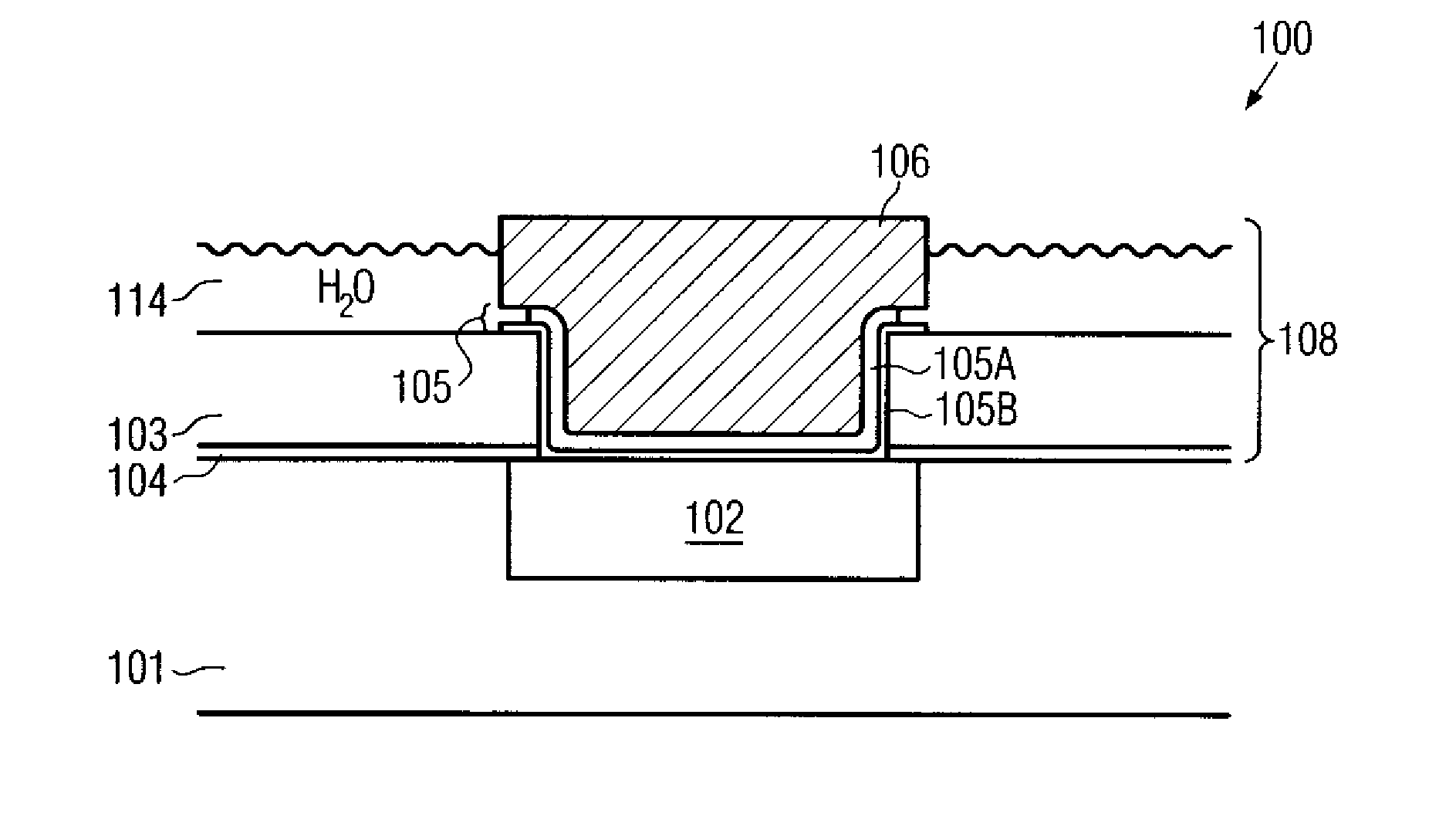
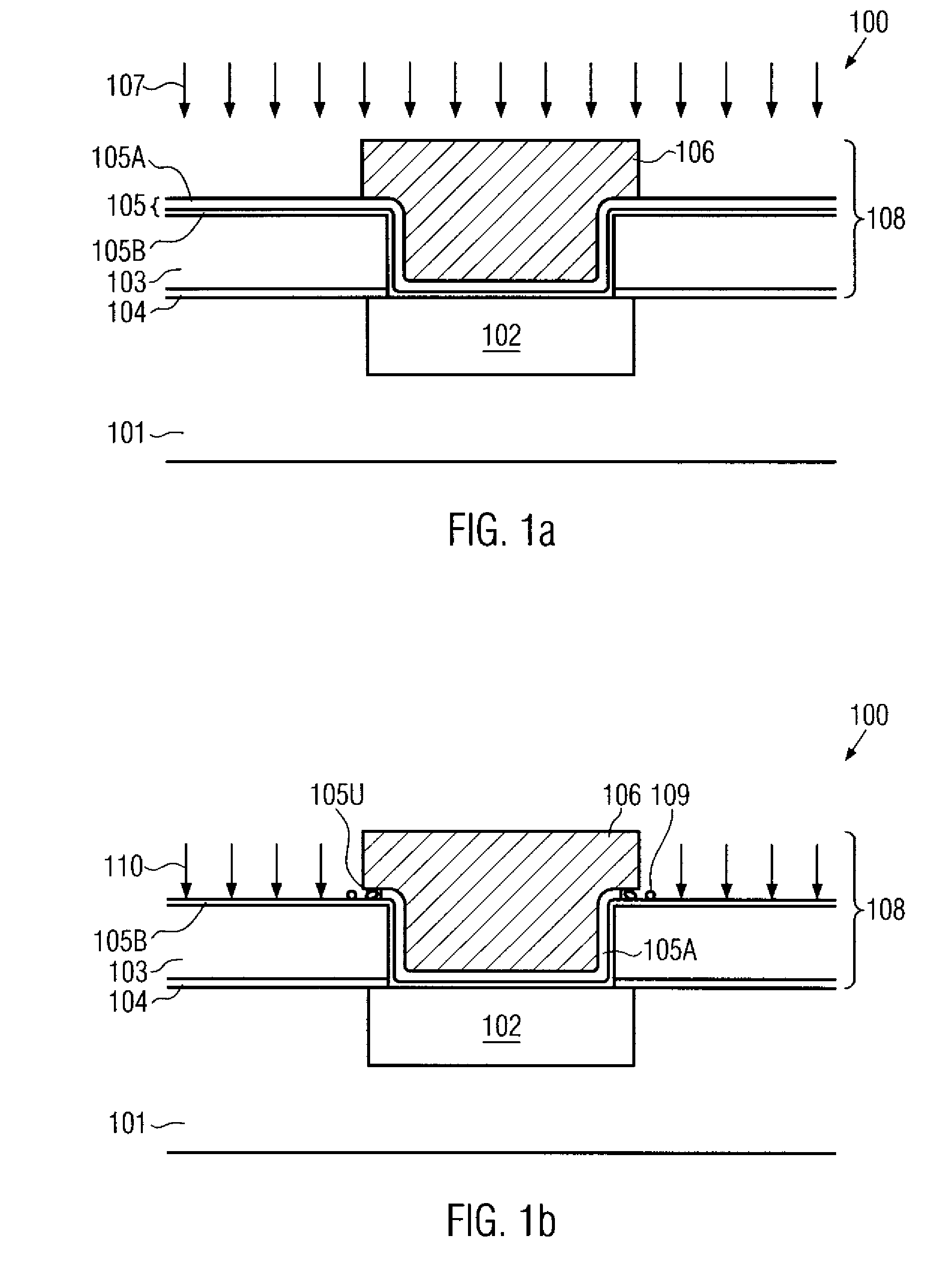
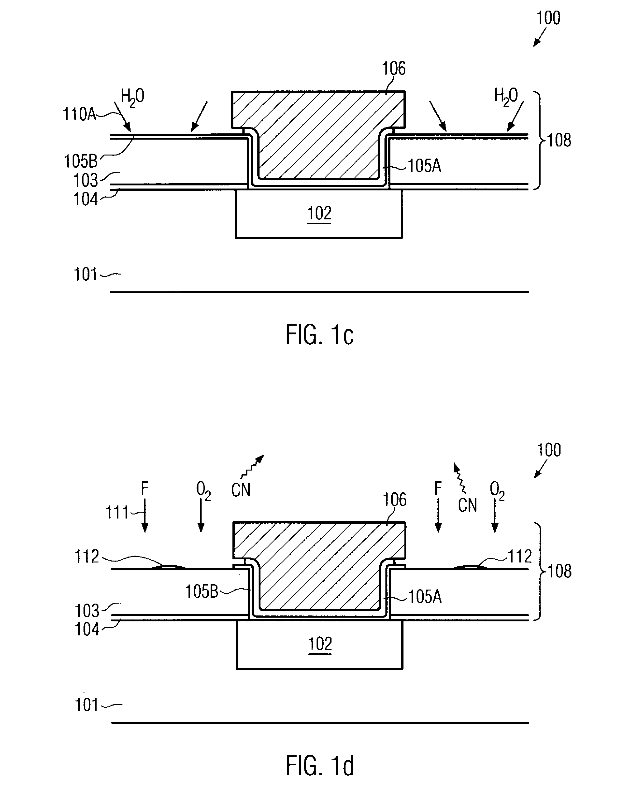
[0019] Illustrative embodiments of the invention are described below. In the interest of clarity, not all features of an actual implementation are described in this specification. It will of course be appreciated that in the development of any such actual embodiment, numerous implementation-specific decisions must be made to achieve the developers' specific goals, such as compliance with system-related and business-related constraints, which will vary from one implementation to another. Moreover, it will be appreciated that such a development effort might be complex and time-consuming, but would nevertheless be a routine undertaking for those of ordinary skill in the art having the benefit of this disclosure.

[0020] The present invention will now be described with reference to the attached figures. Various structures, systems and devices are schematically depicted in the drawings for purposes of explanation only and so as to not obscure the present invention with details that are we...


PUM

PropertyMeasurementUnit
temperatureaaaaaaaaaa
wavelengthaaaaaaaaaa
monitor wavelengthaaaaaaaaaa

Abstract

By patterning the underbump metallization layer stack on the basis of a dry etch process, significant advantages may be achieved compared to conventional techniques involving a highly complex wet chemical etch process. In particular embodiments, a titanium tungsten layer or any other appropriate last layer of an underbump metallization layer stack may be etched on the basis of a plasma etch process using a fluorine-based chemistry and oxygen as a physical component. Moreover, appropriate cleaning processes may be performed for removing particles and residues prior to and after the plasma-based patterning process.

Description

BACKGROUND OF THE INVENTION [0001] 1. Field of the Invention [0002] The present invention generally relates to the formation of integrated circuits, and, more particularly, to a process flow for forming a contact layer including bumps, wherein the contact layer is configured to provide contact areas for directly attaching an appropriately formed package or carrier substrate to a die carrying one or more integrated circuits. [0003] 2. Description of the Related Art [0004] In manufacturing integrated circuits, it is usually necessary to package a chip and provide leads and terminals for connecting the chip circuitry with the periphery. In some packaging techniques, chips, chip packages or other appropriate units may be connected by means of solder balls, formed from so-called solder bumps, that are formed on a corresponding layer, which will be referred to herein as a contact layer, of at least one of the units, for instance on a dielectric passivation layer of the microelectronic chi...

Claims


Application Information

Patent Timeline
Patent Type & Authority Applications(United States)
IPC IPC(8): H01L21/44H01L23/48
CPCH01L24/11H01L24/12H01L2924/07802H01L2224/131H01L2224/11849H01L2224/05671H01L2224/05647H01L2224/05582H01L2224/0401H01L2224/03901H01L2224/0381H01L2224/0361H01L24/13H01L2224/03912H01L2224/11912H01L2224/13099H01L2924/01002H01L2924/01013H01L2924/01015H01L2924/01022H01L2924/01027H01L2924/01029H01L2924/01032H01L2924/01033H01L2924/01046H01L2924/01047H01L2924/01073H01L2924/01074H01L2924/01078H01L2924/01079H01L2924/01082H01L2924/014H01L2924/14H01L2924/1433H01L2924/19043H01L2924/30105H01L2924/01005H01L2924/01006H01L2924/01019H01L2924/01023H01L2924/01024H01L2924/01014H01L2924/0105H01L2924/01057H01L21/02071H01L21/32134H01L24/03H01L24/05H01L2924/00014H01L2924/00H01L23/48H01L23/485
Inventor KUECHENMEISTER, FRANKPLATZ, ALEXANDERJUNGNICKEL, GOTTHARDSIURY, KERSTIN
Owner TAIWAN SEMICON MFG CO LTD
Why Eureka
Try Eureka