Display panel and method of manufacturing same

Inactive Publication Date: 2021-10-28
SHENZHEN CHINA STAR OPTOELECTRONICS SEMICON DISPLAY TECH CO LTD
View PDF0 Cites 0 Cited by
  • Summary
  • Abstract
  • Description
  • Claims
  • Application Information

AI Technical Summary

Benefits of technology

[0016]Beneficial effects of the present application are that: compared with the prior art, in the display panel and the method of manufacturing the same provided by the present invention, the source/drain metal layer of the TFT device is set as a superimposed layer of a transparent metal layer and a non-ferrous metal layer, and the transparent metal layer is extended to

Problems solved by technology

This can solve technical problems that a number of photomasks in a manufacturing process of

Method used


Image

  • Display panel and method of manufacturing same
  • Display panel and method of manufacturing same
  • Display panel and method of manufacturing same

Examples


Embodiment Construction

[0019]Aiming at technical problems that a number of photomasks in a display panel manufacturing process of the prior art is large, which is not conducive to saving production costs, this embodiment can solve this defect.

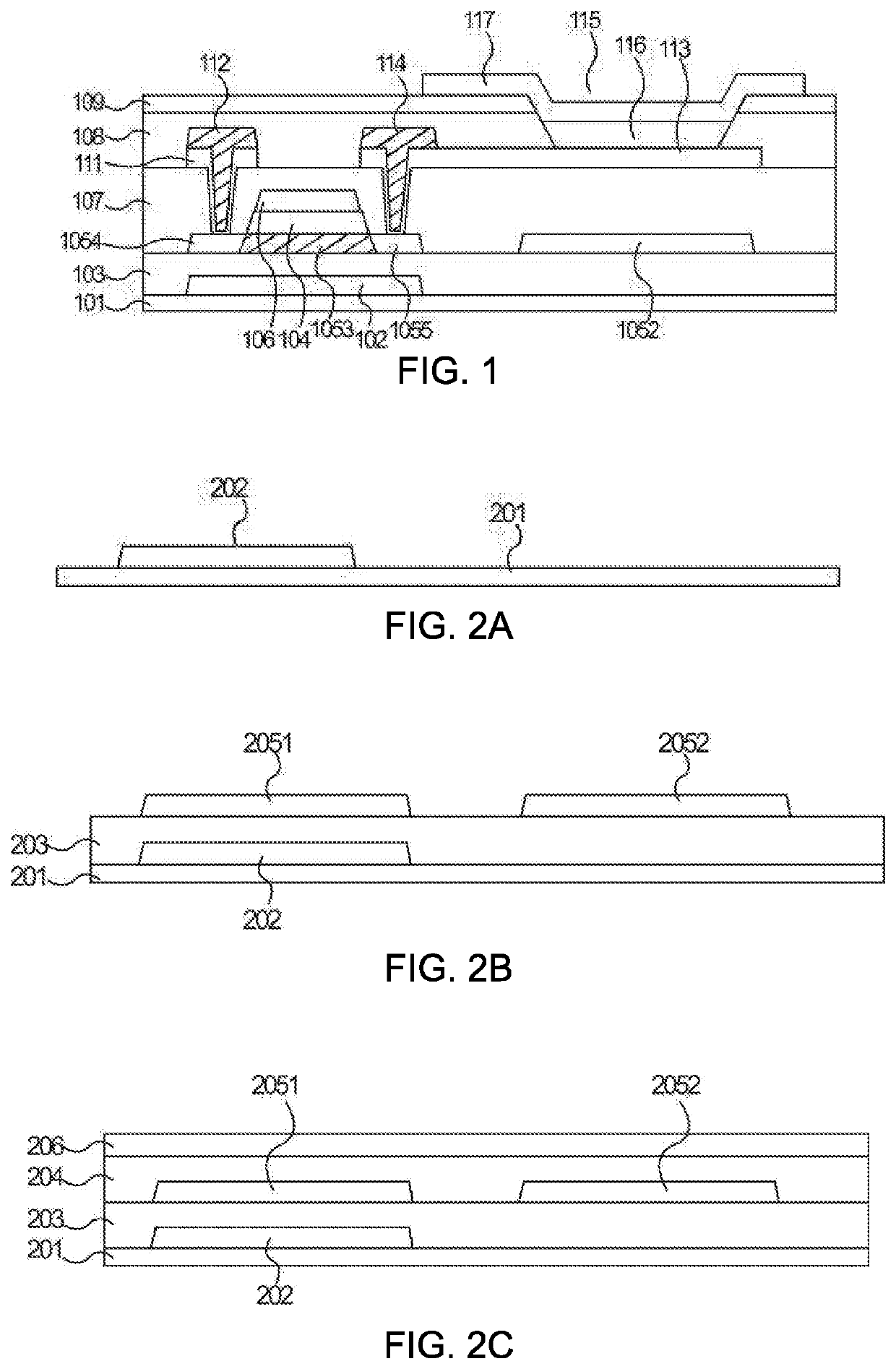
[0020]As shown in FIG. 1, taking an organic light emitting diode (OLED) display panel as an example, a display panel provided by an embodiment of the present invention includes an array of pixel units, and the pixel units include a control area for setting a thin film transistor (TFT) device and a light emitting area for setting an OLED device.

[0021]The control area includes a patterned light shielding layer 102 formed on a surface of a transparent substrate 101, a buffer layer 103 covering the light shielding layer 102, a semiconductor layer (active layer) formed on the buffer layer 103, a gate insulating layer 104 disposed on a surface of the semiconductor layer, a gate 106 disposed on a surface of the gate insulating layer 104, an interlayer insulating layer 107 f...


PUM


Abstract

A display panel is provided. The display panel includes thin film transistors arranged in an array. A source and a drain of each of the thin film transistors each include an electrode layer, and the electrode layer of the source or the drain extends to a pixel opening area and can be used as a pixel electrode.

Description

FIELD OF INVENTION[0001]The present disclosure relates to the field of display technologies, and more particularly to a display panel and a method of manufacturing the same.BACKGROUND OF INVENTION[0002]Organic light emitting diode (OLED) displays are gradually becoming the mainstream of the display industry due to their advantages such as wide viewing angles, high color gamut, and low power consumption.[0003]Currently, thin film transistors (TFTs) prepared with a metal oxide semiconductor as a channel layer have been widely used in organic light emitting diode (OLED) display panels. Top-gate TFTs have become the industry's first choice due to their small parasitic capacitance. However, there are many photomask manufacturing processes required to prepare a top-gate TFT array substrate. The current technology requires 8 or more photomasks, and the cost is high.[0004]In summary, in a manufacturing process of the OLED display panel in the prior art, a number of photomasks is large, whic...

Claims


Application Information

Patent Timeline
IPC IPC(8): H01L27/32G02F1/1368H01L51/52G02F1/1362
CPCH01L27/3272G02F1/1368H01L51/5234H01L2251/308G02F1/136209H01L2227/323H01L27/3265H01L27/1214H01L27/1259G02F1/134309H10K59/12H10K59/1201G02F1/13685G02F1/13439G02F1/1343H01L27/124H01L27/1225H10K59/123H10K59/1216H10K71/00H10K59/126H10K50/828H10K2102/103
Inventor LIN, ZHENGUOZHOU, XINGYUHSU, YUANJUN
Owner SHENZHEN CHINA STAR OPTOELECTRONICS SEMICON DISPLAY TECH CO LTD
Why Eureka
Try Eureka