System and method for reducing current in a device during testing

a technology of electronic devices and current reduction, applied in the field of system and method for testing electronic devices, can solve the problems of reducing costs, increasing complexity of electrical and computing systems that utilize microelectronic devices, and insufficient testing current maximum that can be provided by typical testers,

Active Publication Date: 2007-05-15
NXP USA INC
View PDF10 Cites 0 Cited by
  • Summary
  • Abstract
  • Description
  • Claims
  • Application Information

AI Technical Summary

Benefits of technology

[0034]The invention further provides a system for testing a microelectronic assembly. The system includes a microelectronic device including first transistors and second transistors, a power supply electrically connected to the first and second transistors to provide power to the first and second transistors such that current flows through the first and second transistors, a switch in operable communication with the second transistors, the switch allowing current to flow from the power supply through the second transistors when in a first mode of operation and preventing current from flowing from the power supply through the second transistors when in a second mode of operation, control circuitry in operable communication with the switch, and current sensing circuitry coupled to the first transistors to detect a test amount of current flowing through at least one of the first transistors when the switch is in the first mode of operation.

Problems solved by technology

In recent years, electrical and computing systems that utilize microelectronic devices, such power integrated circuits (IC), have become increasingly complicated.
However, the maximum testing current that can be provided by typical tester is insufficient to fully test some modern devices.
For example, some modern power ICs have channels capable of handling maximum peak currents of over 15 A, while most testers are not able to provide more than 10 A. Therefore, multiple testers are often connected in parallel to provide a sufficient amount of current for fully testing such devices.
However, the use of multiple testers defeats the goal of minimizing costs, as more testers are required within the system, which again increases testing costs.
Additionally, high current operation considerably raises the temperature of the devices, which reduces the longevity and reliability of the devices.

Method used


Image

  • System and method for reducing current in a device during testing
  • System and method for reducing current in a device during testing
  • System and method for reducing current in a device during testing

Examples


Embodiment Construction

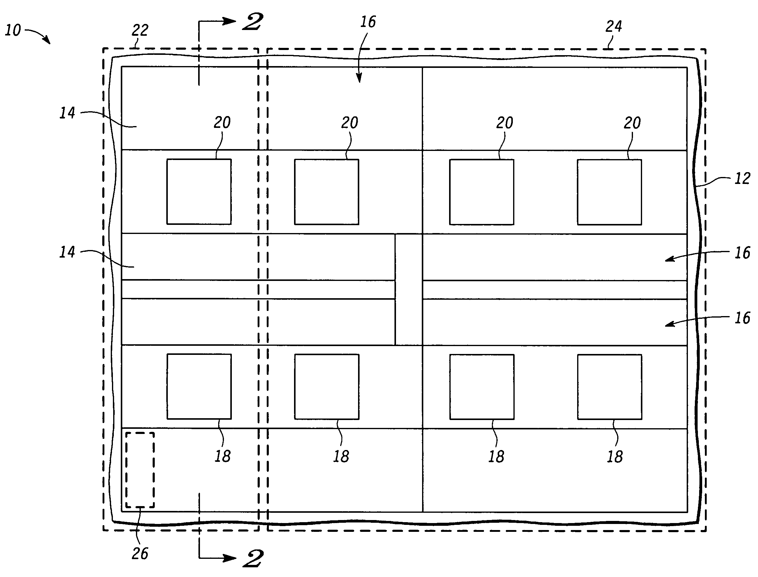
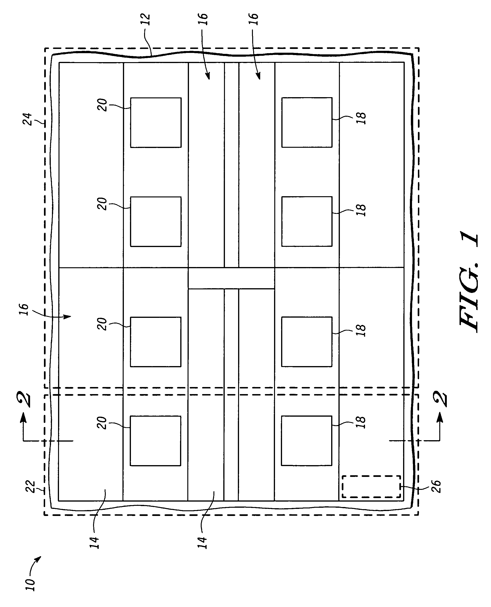
[0011]The following detailed description is merely exemplary in nature and is not intended to limit the invention or application and uses of the invention. Furthermore, there is no intention to be bound by any expressed or implied theory presented in the preceding technical field, background, brief summary, or the following detailed description. It should also be noted that FIGS. 1–4 are merely illustrative and may not be drawn to scale.

[0012]FIGS. 1–4 illustrate a system and method for testing electronic devices using a reduced amount of current. In a first mode of operation, power is provided to the entire device such that a first amount of current flows therethrough. A preferred portion of the device is electrically isolated from a remainder of the device. Power is then provided to the device such that a reduced amount of current flows only through the preferred portion of the electronic assembly. Because the sizes of the conductors within the device are known, the entire device ...


PUM


Abstract

A method for testing an electronic assembly (10) is provided. A portion (22) of the electronic assembly is electrically isolated from a remainder (24) of the electronic assembly. Power is provided to the electronic assembly such that a reduced amount of current flows only through the portion of the electronic assembly. The reduced amount of current is determined. A combined amount of current flowing through both the portion and the remainder of the electronic assembly when power is provided to both the portion and the remainder of the electronic assembly is calculated based on the reduced amount of current.

Description

FIELD OF THE INVENTION[0001]The present invention generally relates to a system and method for testing electronic devices, and more particularly relates to a system and method for testing such devices using a reduced amount of current.BACKGROUND OF THE INVENTION[0002]In recent years, electrical and computing systems that utilize microelectronic devices, such power integrated circuits (IC), have become increasingly complicated. In order to protect various components used in a wide variety of systems, such as automobiles and the like, self-testing features (i.e., built-in testing apparatuses or “testers”) are often provided which allow the microelectronic devices to be tested for appropriate shut off current levels.[0003]In order to minimize costs, multiple devices are often tested simultaneously by the same tester, or testers. However, the maximum testing current that can be provided by typical tester is insufficient to fully test some modern devices. For example, some modern power I...

Claims


Application Information

Patent Timeline
Patent Type & Authority Patents(United States)
IPC IPC(8): G01R31/08G01R31/26
CPCG01R31/2884
Inventor BENNETT, PAUL T.GRAY, RANDALL C.
Owner NXP USA INC
Why Eureka
Try Eureka