Method for tuning an embedded capacitor in a multilayer circuit board

a multi-layer circuit board and embedded capacitor technology, applied in the direction of electrolytic capacitors, variable capacitors, conductive pattern formation, etc., can solve the problems of capacitors consuming the surface area of circuit boards, capacitors frequently introduce undesirable inductance, and preventing the connection of other surface devices, so as to reduce reduce the capacitance, and increase the conductive surface area

Inactive Publication Date: 2007-05-22
RPX CLEARINGHOUSE
View PDF9 Cites 61 Cited by
  • Summary
  • Abstract
  • Description
  • Claims
  • Application Information

AI Technical Summary

Problems solved by technology

Discrete capacitors frequently introduce undesirable inductance from the vias and solder joints used to connect the discrete capacitors to the circuit.
Discrete capacitors also consume the circuit board's surface area, preventing the connection of other surface devices.
For all of their benefits over discrete capacitors, the capacitive values of embedded capacitors often are not as consistent as those of discrete capacitors.
While discrete capacitors may be manufactured to have a predictable capacitance with slight variation, embedded capacitors often have unpredictable capacitances resulting from the circuit board manufacturing processes.
This problem is compounded once the embedded capacitor is laminated inside the substrate of the circuit board because conventional capacitance tuning techniques typically cannot be employed.
As a result, when a circuit board having an embedded capacitor with inadequate capacitance is detected, conventional techniques typically call for adjusting the nominal capacitance by adding a surface mount capacitor in parallel, thereby introducing the undesirable effects of discrete capacitors.
Conventional techniques, however, do not provide for an efficient way to decrease the capacitance of an embedded capacitor having excessive capacitance in a laminated circuit board.
Consequently, the circuit board typically is either used in its present condition, often to ill effect, or it is discarded.

Method used


Image

  • Method for tuning an embedded capacitor in a multilayer circuit board
  • Method for tuning an embedded capacitor in a multilayer circuit board
  • Method for tuning an embedded capacitor in a multilayer circuit board

Examples


Embodiment Construction

)

[0017]The following description is intended to convey a thorough understanding of the present invention by providing a number of specific embodiments and details involving tuning embedded capacitors in printed circuit boards and other circuit devices. It is understood, however, that the present invention is not limited to these specific embodiments and details, which are exemplary only. It is further understood that one possessing ordinary skill in the art, in light of known systems and methods, would appreciate the use of the invention for its intended purposes and benefits in any number of alternative embodiments, depending upon specific design and other needs.

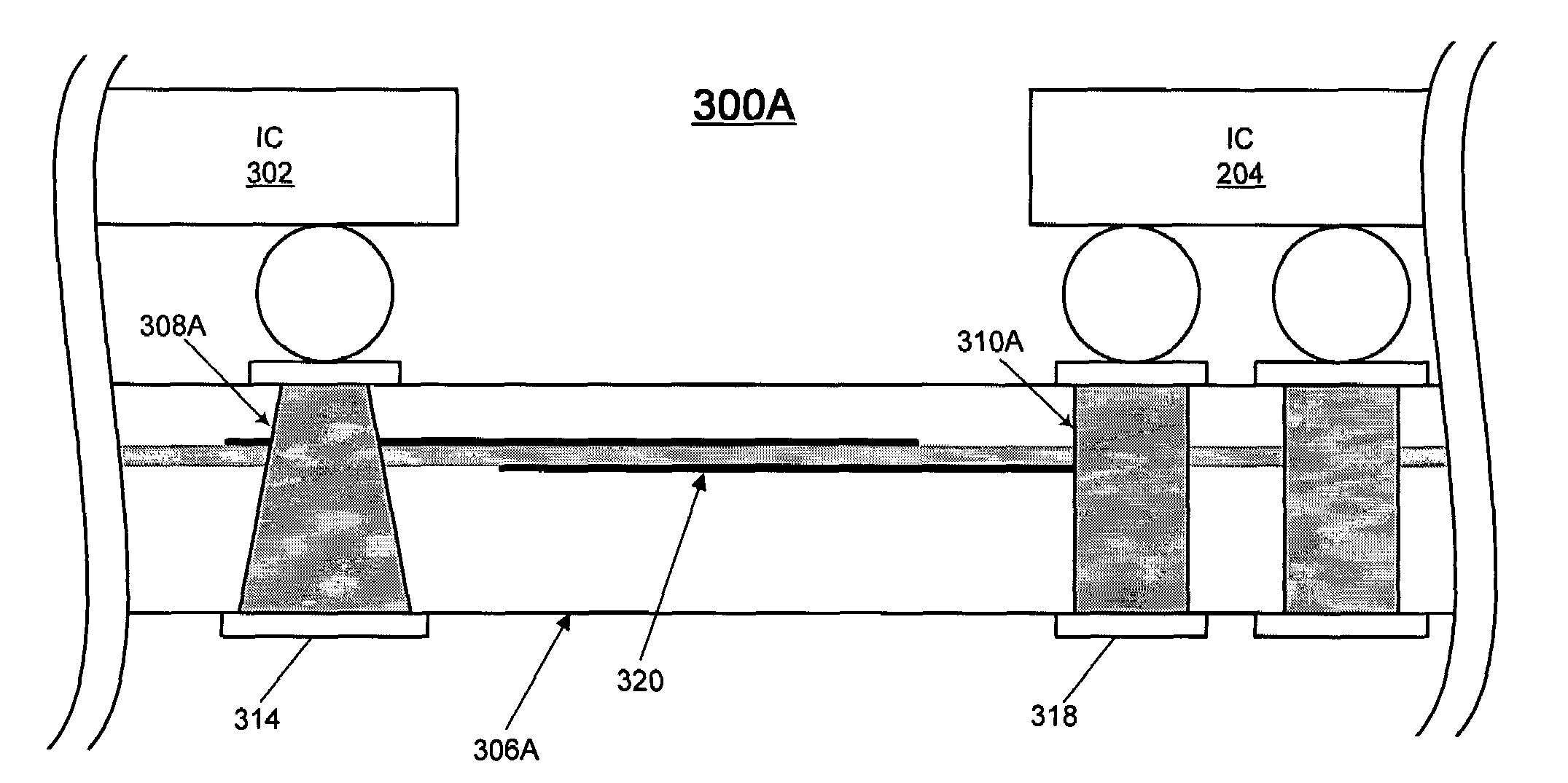
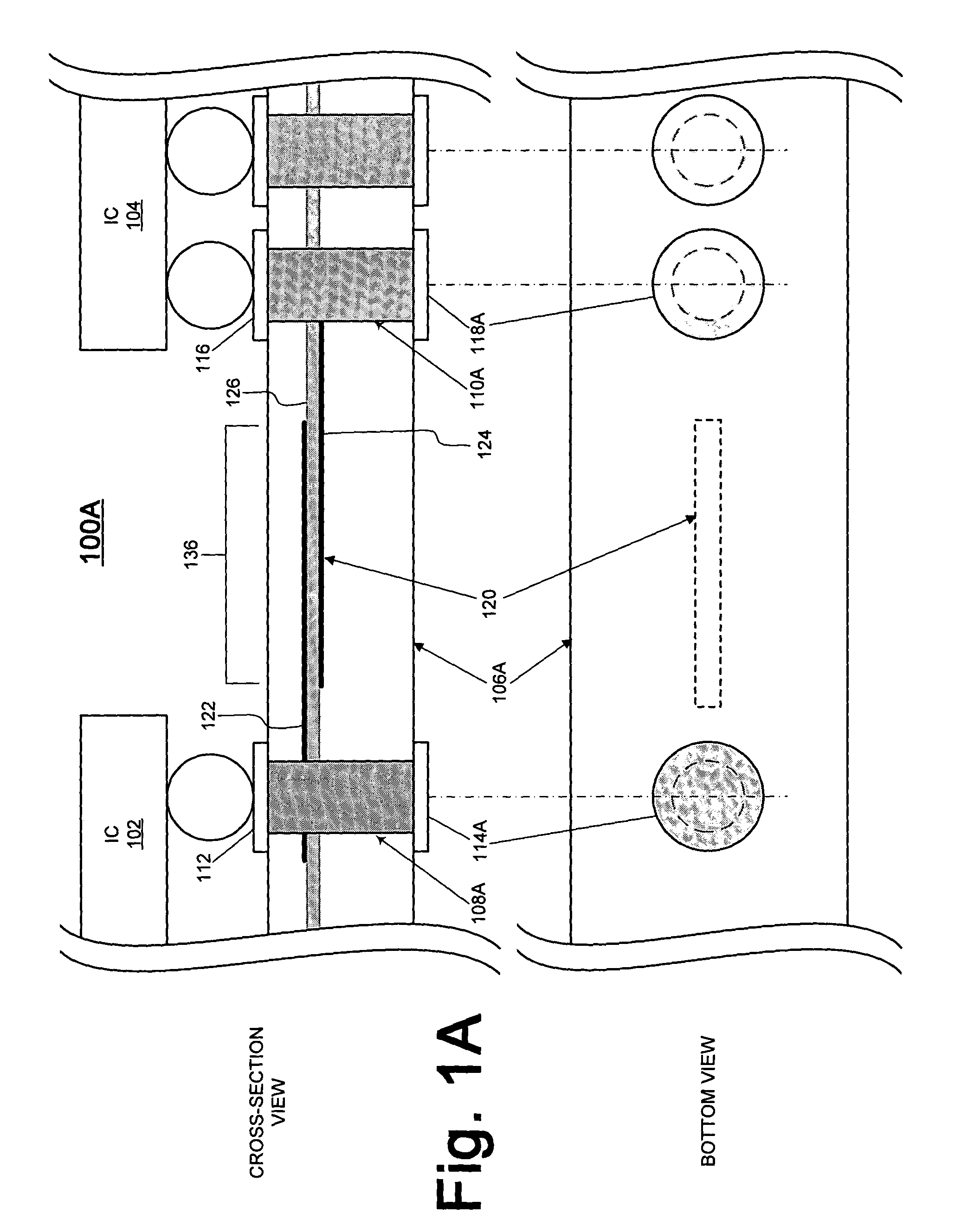
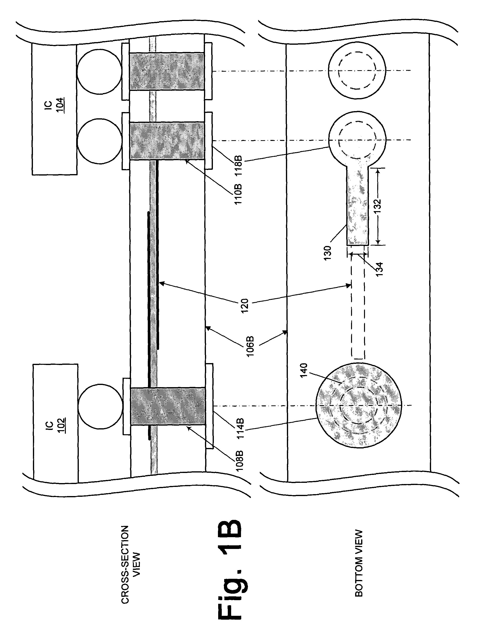
[0018]FIGS. 1A–3B illustrate various exemplary techniques for tuning an embedded capacitor formed in a multilayer circuit board. In at least one embodiment, one or more conductive features of one or more vias connected to the embedded capacitor may be modified to adjust the capacitance contributed by the one or more vias. O...


PUM

PropertyMeasurementUnit
diameteraaaaaaaaaa
surface areaaaaaaaaaaa
capacitanceaaaaaaaaaa

Abstract

Exemplary techniques for tuning the effective capacitance provided by an embedded capacitor are disclosed. The techniques may be realized by modifying one or more conductive features of one or more vias connected to the embedded capacitor to adjust the capacitance contributed by the one or more vias. One technique preferably includes altering the conductive surface area of a pad of one or more vias to which the embedded capacitor is electrically connected to increase or decrease the contributed capacitance. Another technique provides for bore drilling or tap drilling one or more vias connected to the embedded capacitor to increase the surface area of plated interior surfaces of the vias, thereby increasing their capacitive effect. An additional technique includes forming a number of vias having various capacitive effects and electrically connecting the embedded capacitor to one or more of these vias to increase the capacitance.

Description

FIELD OF THE INVENTION[0001]The present invention relates generally to embedded capacitors in multilayer circuit boards and, more particularly, to techniques for tuning the capacitance of an embedded capacitor by modifying one or more features of one or more vias connected thereto.BACKGROUND OF THE INVENTION[0002]Capacitors formed within, or “embedded” in, multilayer circuit boards often are beneficially used in addition to or in place of discrete surface mount (SMT) capacitors. Discrete capacitors frequently introduce undesirable inductance from the vias and solder joints used to connect the discrete capacitors to the circuit. Discrete capacitors also consume the circuit board's surface area, preventing the connection of other surface devices. In contrast, embedded capacitors frequently exhibit less inductance than surface capacitors because of their proximity to the driver and receiver and due to their lack of solder joints and extra vias. Further, because they are embedded in inn...

Claims


Application Information

Patent Timeline
Patent Type & Authority Patents(United States)
IPC IPC(8): H01G9/00H01L27/108
CPCH01L23/49822H05K1/162Y10T29/49156H01L2224/16H01L2924/01078H05K1/113H05K1/116H05K3/0047H05K3/429H05K2201/0959H05K2201/09627H05K2203/0207H05K2203/0242H05K2203/171H05K2203/173H05K2203/175H01L2224/16235H01L2924/01068Y10T29/417Y10T29/49165Y10T29/43Y10T29/435Y10T29/49155H01L25/16
Inventor WYRZYKOWSKA, ANETAKWONG, HERMAN
Owner RPX CLEARINGHOUSE
Why Eureka
Try Eureka