Multi-chips module package and manufacturing method thereof

a technology of modules and modules, applied in the direction of semiconductor devices, electrical equipment, semiconductor/solid-state device details, etc., can solve the problems of reducing the cost of substrates, limiting the development of integrated circuit devices of higher performance, and reducing the distance of transmitting electrical signals, so as to enhance electrical performance, reduce cost, and enhance the effect of electrical performan

Active Publication Date: 2007-05-22
ADVANCED SEMICON ENG INC
View PDF3 Cites 13 Cited by
  • Summary
  • Abstract
  • Description
  • Claims
  • Application Information

AI Technical Summary

Benefits of technology

[0016]In summary, this invention is related to a multi-chips module package with a lead frame therein for electrically connecting the first chip and the second chip to external electronic devices. In such a manner, it not only reduces the distance of transmitting the electrical signals from chips to the outside so as to enhance electrical performance but also it can save cost due to the lead frame manufactured by a simple manufacturing processes.

Problems solved by technology

However, recently, integrated circuits packaging technology is becoming a limiting factor for the development in packaging integrated circuits devices of higher performance.
Semiconductor package designers are struggling to keep pace with the increase in pin count, size limitations, low profile, and other evolving requirements for packaging and mounting integrated circuits.
As mentioned above, the layout of the circuits arranged in the substrate applicable to such package as shown above is so complex that the cost of substrate is very expensive due to the complexity of manufacturing substrate.
Moreover, the electrical traces are longer so that the impedance, the inductance and the noise will be increased to lower the electrical performance.
However, the leads are easily separated from the encapsulation so as to be not able to well connect to external electronic devices.

Method used


Image

  • Multi-chips module package and manufacturing method thereof
  • Multi-chips module package and manufacturing method thereof
  • Multi-chips module package and manufacturing method thereof

Examples


Embodiment Construction

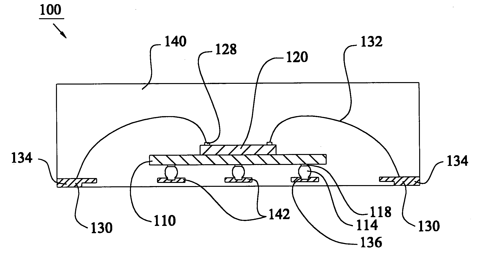
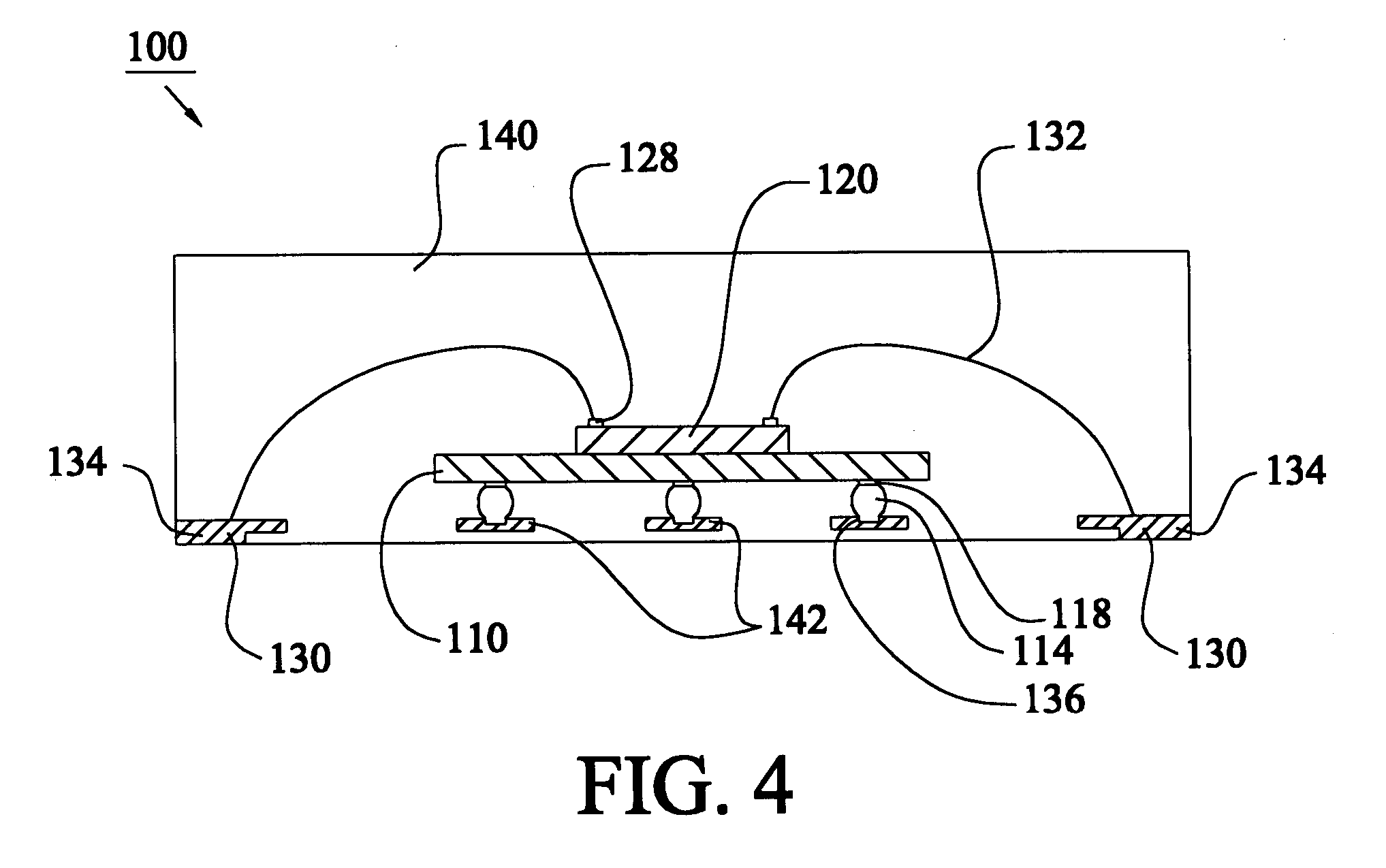
[0035]The multi-chips module package according to the preferred embodiments of this invention will be described herein below with reference to the accompanying drawings, wherein the same reference numbers refer to the same elements.

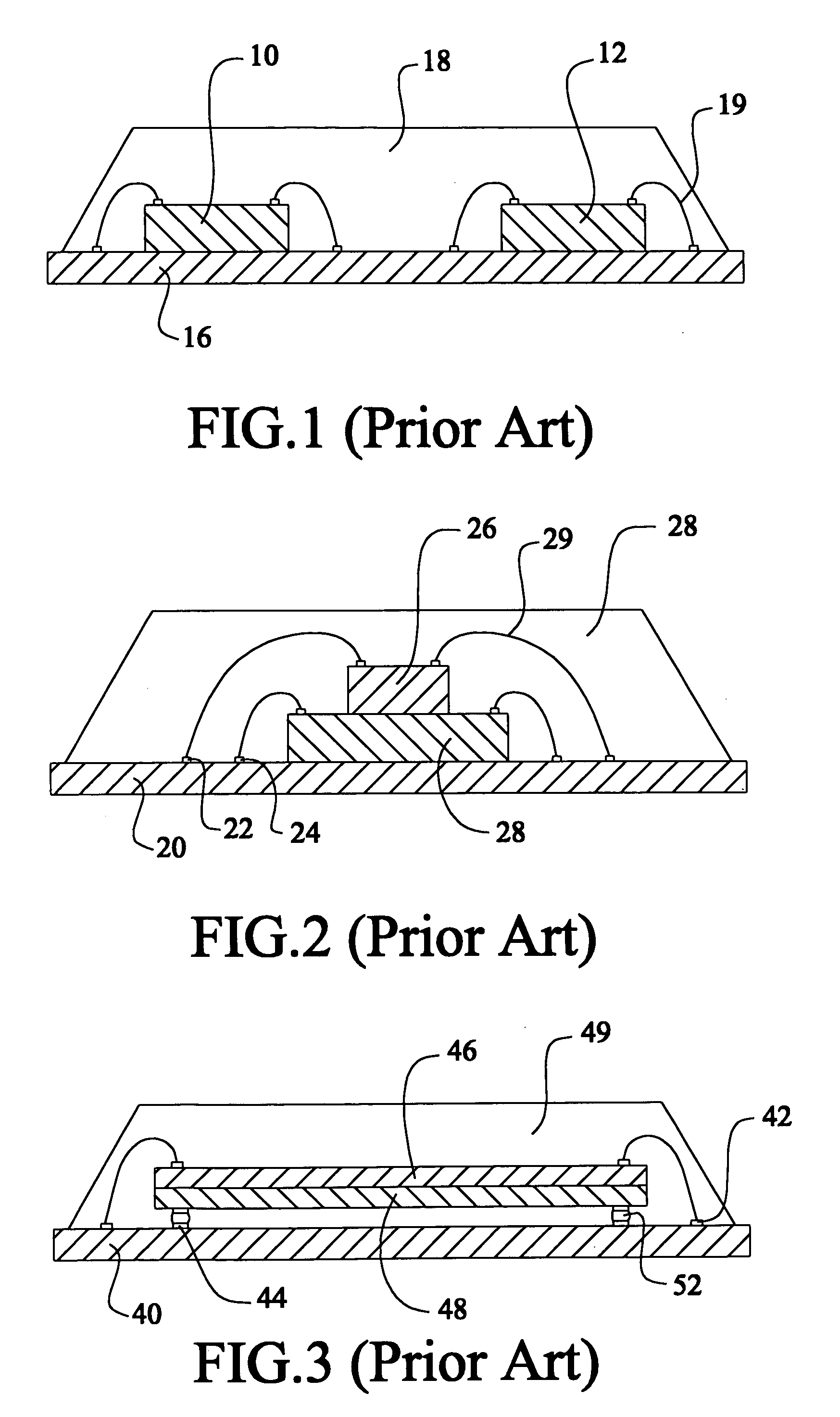
[0036]FIGS. 4 and 5 are enlarged cross-sectional views showing the cross-sectional view of a multi-chips module package according to the first preferred embodiment of this invention.

[0037]As shown in FIG. 4, the multi-chips module package 100 mainly comprises a first chip 110, a second chip 120 and a lead frame 130. Therein, the first chip 110 is flip-chip bonded to the lead fame 130 and the second chip 120 is disposed on the first chip 110 and electrically connected to the lead frame 130 through a plurality of electrically conductive wires.

[0038]To be noted, the lead frame 130 as mentioned above has a plurality of leads 134, chip pads 142 and tie bars 143, wherein at least one of the chip pads 142 is connected to one of the leads 134 through the correspo...


PUM


Abstract

A multi-chips module package comprises a lead frame, a first chip, a second chip, a plurality of electrically conductive wires and an encapsulation. The lead frame has a plurality of first leads, second leads and chip pads connecting to the first leads. The first chip is placed on the lead frame and electrically connected to the lead frame through the bumps connecting the bump-bonding pads and the chip pads and the first leads; the second chip is placed over the first chip and electrically connected to the lead frame through the wires connecting the wire-bonding pads to the second leads; and the encapsulation covers the first chip, the second chip, the lead frame, and the wires. In such a manner, it not only reduces the distance of transmitting the electrical signals from chips to the outside but also it can save cost due to the lead frame manufactured by a simple manufacturing processes. In addition, a manufacturing method of the multi-chips module package is provided.

Description

BACKGROUND OF THE INVENTION[0001]1. Field of Invention[0002]This invention relates to a multi-chips module package. More particularly, the present invention is related to a multi-chips module package for integrating wire-bonded chip and flip chip therein and a manufacturing method thereof.[0003]2. Related Art[0004]As we know, in the semiconductor industries, the manufacture of semiconductors mainly comprises the manufacture of wafers and the assembly of integrated circuits devices. Therein, the integrated circuits (ICs) devices are completely formed by the processes of forming integrated circuits devices on the semiconductor wafers, sawing the wafers into individual integrated circuits devices, placing the individual integrated circuits devices on the substrates, electrically connecting the integrated circuits devices to the substrates respectively and encapsulating the integrated circuits devices and substrates to form a plurality of individual assembly packages. Due to the encapsu...

Claims


Application Information

Patent Timeline
Patent Type & Authority Patents(United States)
IPC IPC(8): H01L23/495H01L23/31
CPCH01L23/3107H01L23/49575H01L24/16H01L24/49H01L24/97H01L2224/13099H01L2224/13144H01L2224/16H01L2224/32145H01L2224/48091H01L2224/48247H01L2224/4911H01L2224/49171H01L2924/01013H01L2924/01027H01L2924/01047H01L2924/01079H01L2924/01082H01L2924/14H01L2924/30107H01L2924/3011H01L2924/00014H01L24/48H01L2924/01033H01L2924/014H01L2924/00H01L2224/16245H01L2224/48145H01L2224/73265H01L24/05H01L2224/05554H01L2224/05568H01L2224/05573H01L2224/97H01L2924/10162H01L2924/181H01L2224/45099H01L2224/05599H01L2924/00012
Inventor LIN, CHIAN-CHICHANG, CHIH-HUANG
Owner ADVANCED SEMICON ENG INC
Why Eureka
Try Eureka