Azimuthal scanning of a structure formed on a semiconductor wafer

a semiconductor wafer and scanning technology, applied in the field of optical metrology, can solve the problems of mis-fitting between measured signals, measurement errors, and more complex optical metrology of 3-d structures

Inactive Publication Date: 2007-05-29
TOKYO ELECTRON LTD
View PDF23 Cites 47 Cited by
  • Summary
  • Abstract
  • Description
  • Claims
  • Application Information

AI Technical Summary

Problems solved by technology

However, when performing optical metrology on a structure, measurement errors may occur if the structure and the incident beam are not properly aligned azimuthally.
In particular, cross polarization components of the diffracted beam may complicate the signal measurements, and cause mis-fitting between the measured signals and the analysis model used in optical metrology.
Due to the additional dimension compared to two dimensional (2-D) structures, such as lines / spaces, performing optical metrology of 3-D structures is more complex.

Method used


Image

  • Azimuthal scanning of a structure formed on a semiconductor wafer
  • Azimuthal scanning of a structure formed on a semiconductor wafer
  • Azimuthal scanning of a structure formed on a semiconductor wafer

Examples


Embodiment Construction

[0022]The following description sets forth numerous specific configurations, parameters, and the like. It should be recognized, however, that such description is not intended as a limitation on the scope of the present invention, but is instead provided as a description of exemplary embodiments.

1. Optical Metrology

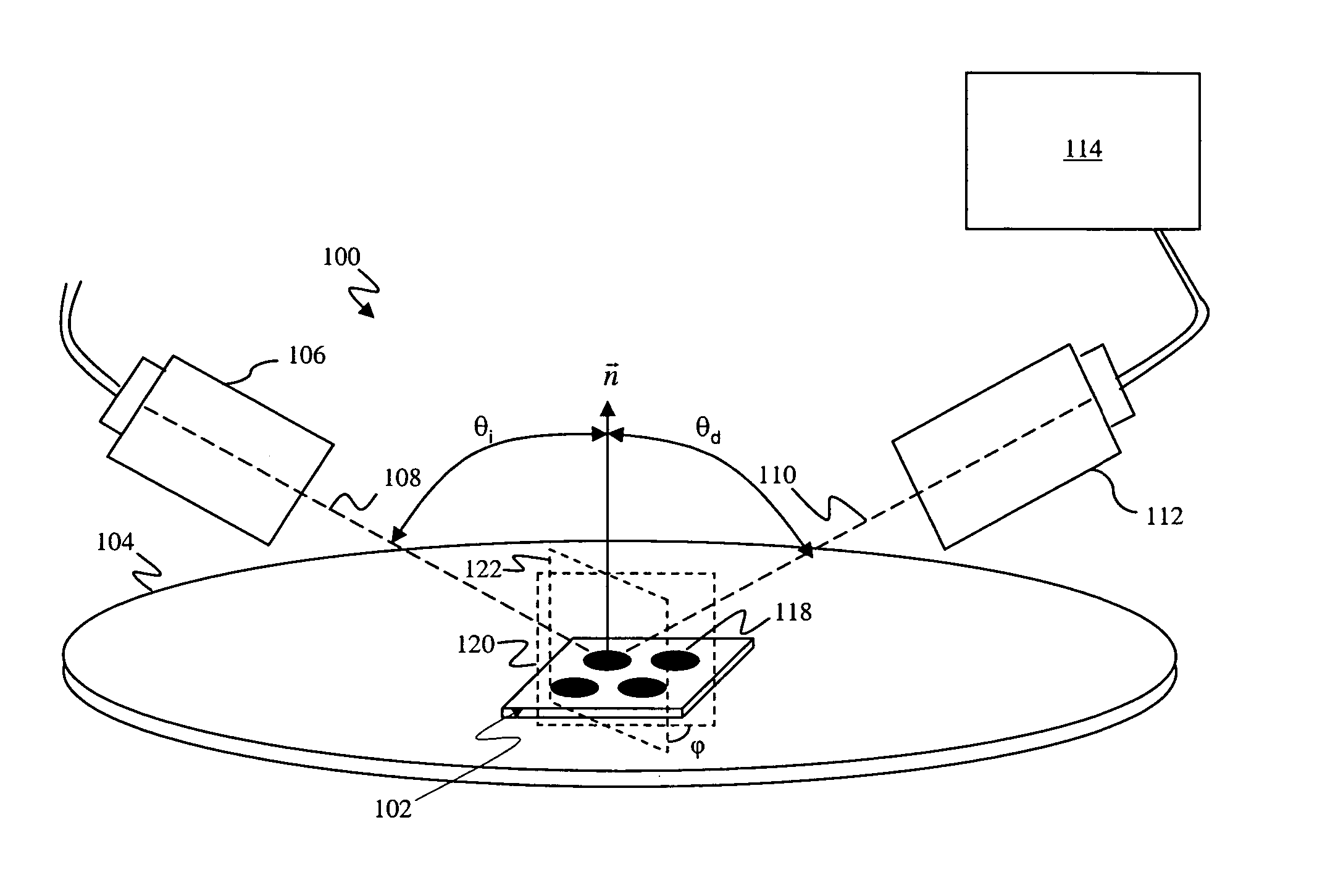
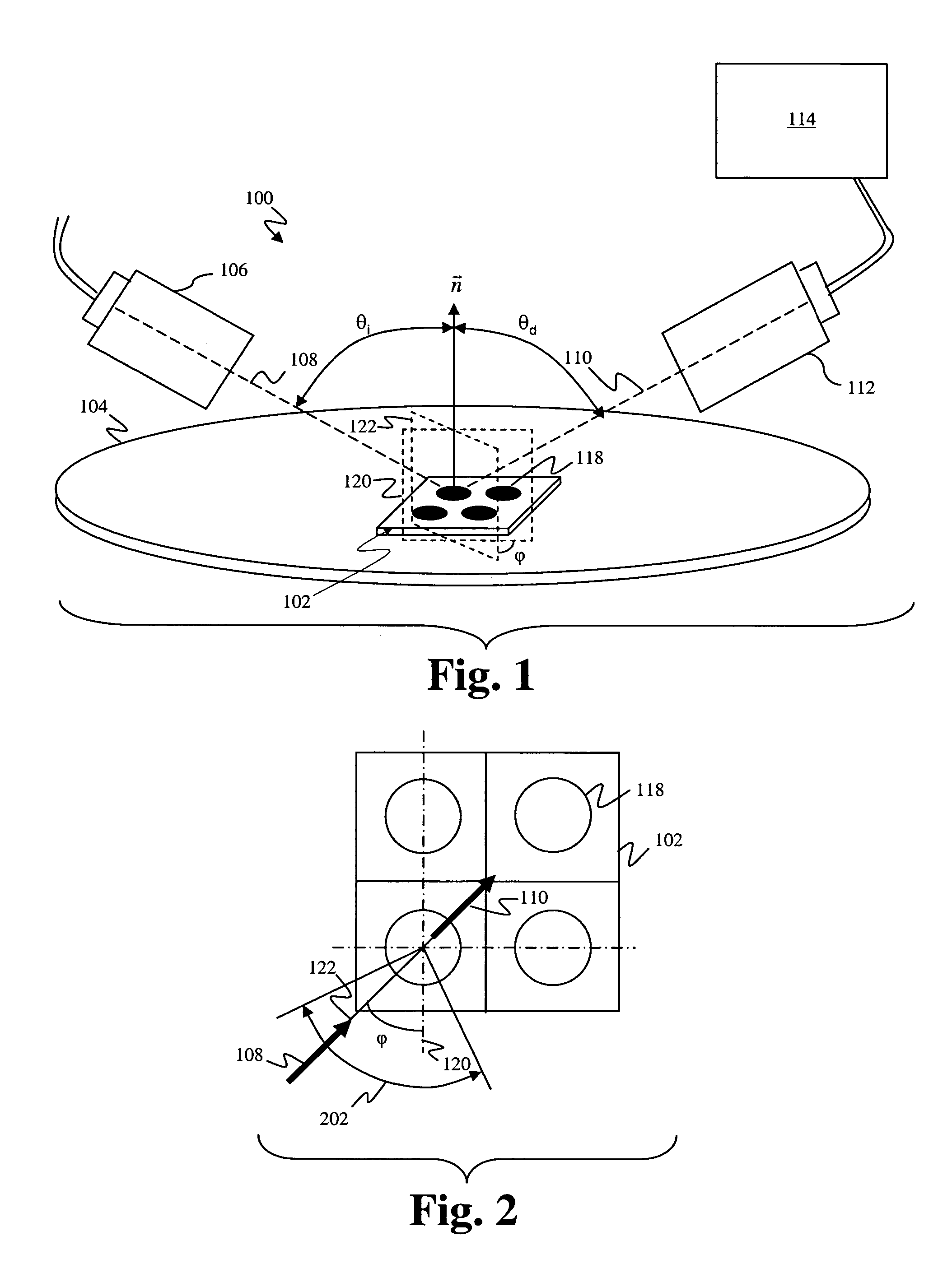
[0023]With reference to FIG. 1, an optical metrology system 100 can be used to examine and analyze a 3-D structure formed on a semiconductor wafer. For example, optical metrology system 100 can be used to determine a feature of a grating array 102 formed on wafer 104. As described earlier, grating array 102 can be formed in test areas on wafer 104, such as adjacent to a device formed on wafer 104. Alternatively, grating array 102 can be formed in an area of the device that does not interfere with the operation of the device or along scribe lines on wafer 104. Although grating array 102 is depicted in FIG. 1 as a contact hole array, it should be recognized that grating arra...


PUM

PropertyMeasurementUnit
polarization angleaaaaaaaaaa
azimuth angleaaaaaaaaaa

Abstract

A structure formed on a semiconductor wafer is examined by directing an incident beam at the structure at an incidence angle and a azimuth angle. The incident beam is scanned over a range of azimuth angles to obtain an azimuthal scan. The cross polarization components of diffracted beams are measured during the azimuthal scan.

Description

BACKGROUND[0001]1. Field of the Invention[0002]The present application relates to optical metrology, and more particularly to azimuthal scanning of a structure formed on a semiconductor wafer.[0003]2. Related Art[0004]Optical metrology involves directing an incident beam at a structure, measuring the resulting diffracted beam, and analyzing the diffracted beam to determine a feature of the structure. In semiconductor manufacturing, optical metrology is typically used for quality assurance. For example, after fabricating a grating array in proximity to a semiconductor chip on a semiconductor wafer, an optical metrology system is used to determine the profile of the grating array. By determining the profile of the grating array, the quality of the fabrication process utilized to form the grating array, and by extension the semiconductor chip proximate the grating array, can be evaluated.[0005]However, when performing optical metrology on a structure, measurement errors may occur if th...

Claims


Application Information

Patent Timeline
Patent Type & Authority Patents(United States)
IPC IPC(8): G01B11/24G01J4/00G01N21/956H01L
CPCG01N21/956G01B11/24G01B11/30
Inventor BISCHOFF, JOERGLI, SHIFANGNIU, XINHUI
Owner TOKYO ELECTRON LTD
Why Eureka
Try Eureka