Semiconductor device and method and apparatus for testing such a device

a technology of mikro-conductor and scan vector, which is applied in the direction of error prevention, digital transmission, instruments, etc., can solve the problems of accidental or malicious use of incorrect scan vector, incorrect input scan vector has somehow become corrupted, etc., and achieves a high degree of reassurance and further enhanced security

Active Publication Date: 2007-06-05
ORACLE INT CORP
View PDF10 Cites 7 Cited by
  • Summary
  • Abstract
  • Description
  • Claims
  • Application Information

AI Technical Summary

Benefits of technology

[0042]A particular advantage of the digital signature approach is that the signature is calculated from the (operative) input scan vector itself. Thus the signature serves as a direct confirmation that the correct input scan vector is being used, since any change or corruption of the input scan vector will lead to a different (incorrect) digital signature being calculated, and hence a lack of authorisation.
[0043]Security can be further enhanced by storing a public key on the device. This public key corresponds to a private key of an asymmetric encryption algorithm used to initially gen

Problems solved by technology

As previously described, the semiconductor device may include a component that is vulnerable to potential damage during scan testing with a given input data configuration.
Thus if the input scan vector does not satisfy the predetermined criterion (or criteria), it is regarded as not properly authorised.
This may occur fo

Method used


Image

  • Semiconductor device and method and apparatus for testing such a device
  • Semiconductor device and method and apparatus for testing such a device
  • Semiconductor device and method and apparatus for testing such a device

Examples


Embodiment Construction

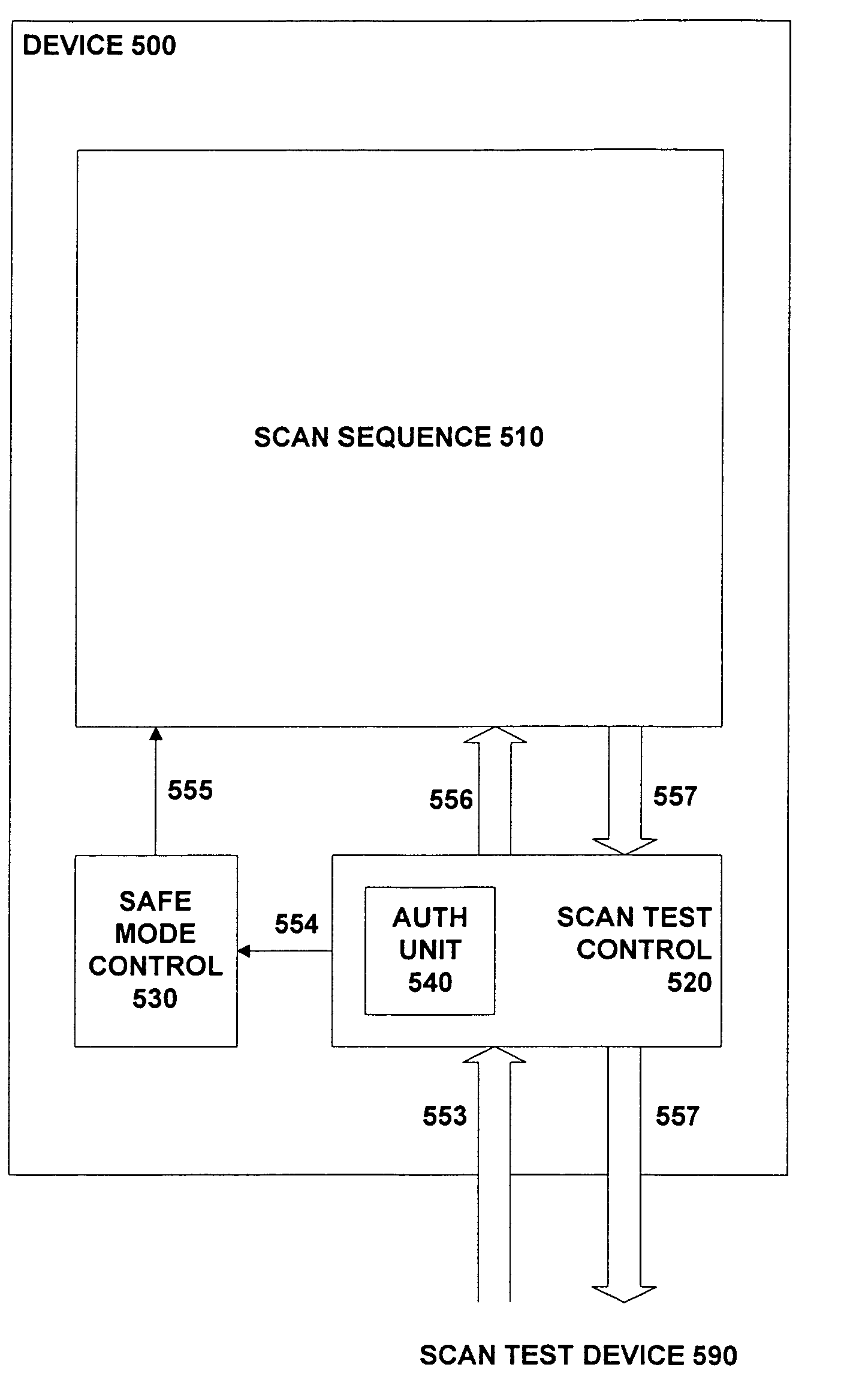
[0068]FIG. 5 depicts a semiconductor device 500 that supports scan testing in accordance with one embodiment of the invention. Thus device 500 includes a scan test control unit 520, which interacts with an external scan test device 590. This interaction is typically performed via appropriate input / output pins on device 500, such as by using a JTAG connection (as described in more detail below, with reference to FIG. 14).

[0069]Semiconductor device 500 also includes a scan sequence 510. This represents the set of functional components on the device that are joined together to form the sequence of flip-flops and so on that are to be tested in scan mode. Thus to perform such testing, the scan test control unit 520 receives an input scan vector 553 from external scan test device 590, along with appropriate control commands. This input scan vector is then forwarded to the scan sequence 510, as indicated by arrow 556. One or more processing steps are then performed within the scan sequence...


PUM


Abstract

A semiconductor device includes at least one component which is vulnerable to damage during scan testing for a particular input data configuration, and supports a safe mode in which this particular input data configuration is disabled. The semiconductor device also includes a port for receiving an input scan vector for scan testing, and an authorization unit connected to said port. The authorization unit maintains the device in safe mode if an input scan vector does not satisfy at least one predetermined criterion. In one particular implementation, the authorization unit generates a digital signature for the input scan vector, which is then compared to a signature portion included within the input scan vector itself. Scan testing is enabled providing that this comparison finds a match.

Description

RELATED APPLICATION[0001]The present application is related to the U.S. patent application Ser. No. 10 / 337,573 (assignee reference number P6588), filed concurrently herewith, and sharing the same title, inventors, and assignee as the present application, the teachings of which are incorporated by reference herein.FIELD OF THE INVENTION[0002]The present invention relates to semiconductor devices, and in particular to the testing of such devices.BACKGROUND OF THE INVENTION[0003]Modern computer systems typically involve many components interacting with one another in a highly complex fashion. For example, a server installation may have multiple processors, configured either within individual (uniprocessor) machines, or combined into one or more multiprocessor machines. Such computer systems operate in conjunction with associated memory and disk drives for storage, video terminals and keyboards for input / output, plus interface facilities for data communications over one or more networks...

Claims


Application Information

Patent Timeline
IPC IPC(8): G01R31/28H04L1/00G01R31/317G01R31/3185G06F11/267
CPCG01R31/31719G01R31/318552G06F11/267
Inventor WILLIAMS, EMRYSHOUSE, KENNETH ALANSIEGEL, JOSEPH RAYMOND
Owner ORACLE INT CORP
Why Eureka
Try Eureka