Semiconductor integrated circuit device and wireless communication system

a technology of integrated circuit and wireless communication system, which is applied in the direction of amplifier combination, gain control, transmission, etc., can solve problems such as signal distortion

Inactive Publication Date: 2007-06-19
RENESAS ELECTRONICS CORP
View PDF8 Cites 12 Cited by
  • Summary
  • Abstract
  • Description
  • Claims
  • Application Information

AI Technical Summary

Benefits of technology

[0004]In comparison of a step amplifier with a linear amplifier, the linear amplifier exhibits large fluctuation of power consumption because gain is varied with current, but the step amplifier has a merit that power consumption of battery can be reduced in the system driven with a battery because power consumption does not change to a large extent even if gain is varied. Moreover, the linear amplifier has a disadvantage that the gain control range is narrower than that of the step amplifier and the amplifier may be saturated in the high-gain range to result in distortion of signal.
[0008]An object of the present invention is to provide a semiconductor integrated circuit device to form a wireless communication system of the dual or more modes including the W-CDMA system which can use a step amplifier as the gain control amplifier to amplify the reception signal, thereby to keep power consumption to almost constant value even when the gain is changed depending on the intensity of reception signal and to assure longer battery life in the portable telephone, namely longer reception waiting period and communication period through single charging process.
[0009]Another object of the present invention is to provide a semiconductor integrated circuit device and a wireless communication system using the same circuit device which can widen the gain control range of gain control amplifier to amplify the reception signal in order to improve the CN ratio.
[0013]According to the means described above, since a step amplifier is used as the gain control amplifier, power consumption can be set almost to the constant value even when the gain is changed depending on the intensity of reception signal and moreover since two step amplifiers are provided to change the gain and the input reception signal is switched after the cancellation of offset, missing of the receiving data due to the offset canceling operation can be eliminated even if the signal can be received continuously.
[0015]According to the means described above, since a step amplifier is used as the gain control amplifier, power consumption can be controlled almost to the constant value even when the gain is changed depending on the intensity of reception signal and moreover in the mode including the function for repairing the receiving data, for example, such as the W-CDMA system, any problem does not occur in the receiving operation because if a part of the receiving data is lost, such missing data can be recovered by switching the gain and canceling the offset during the receiving operation.

Problems solved by technology

Moreover, the linear amplifier has a disadvantage that the gain control range is narrower than that of the step amplifier and the amplifier may be saturated in the high-gain range to result in distortion of signal.

Method used


Image

  • Semiconductor integrated circuit device and wireless communication system
  • Semiconductor integrated circuit device and wireless communication system
  • Semiconductor integrated circuit device and wireless communication system

Examples


embodiment 1

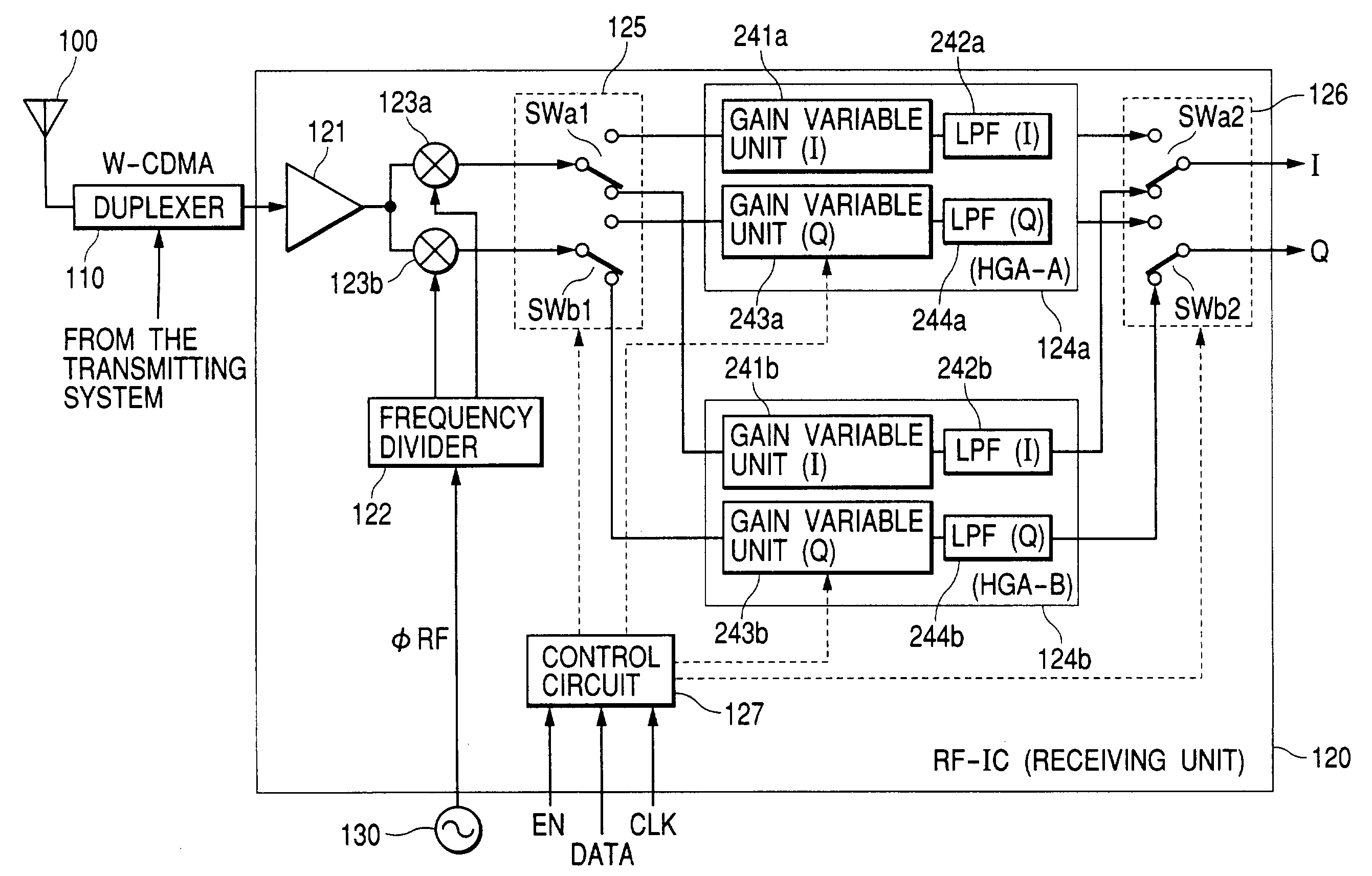
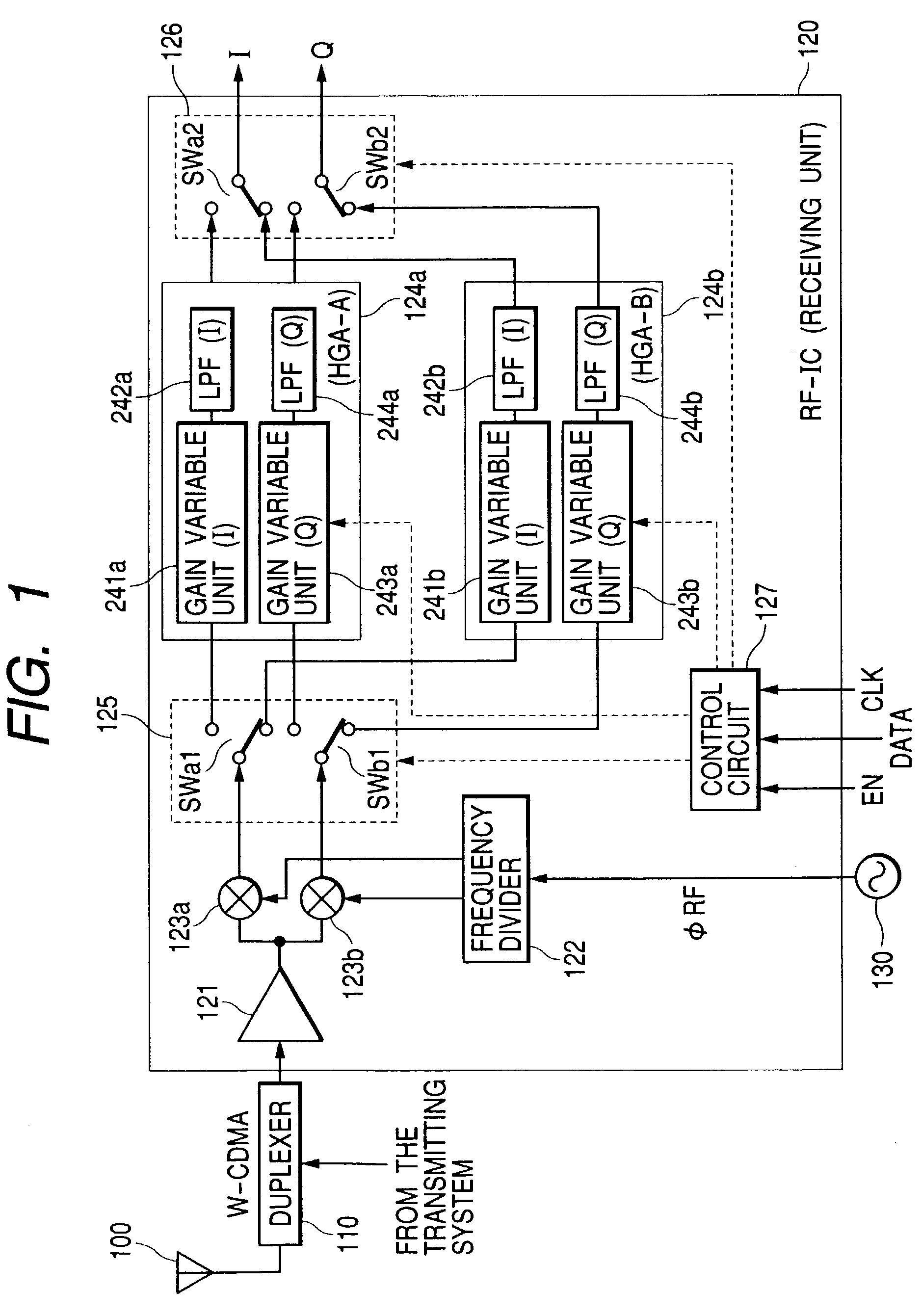
[0029]FIG. 1 illustrates an example of structure of receiving system circuit of portable telephone as the first embodiment to which the present invention is suitably applied. Although not particularly restricted, this embodiment can be suitably applied to a communication system for continuously receiving the reception signal of the W-CDMA system.

[0030]In FIG. 1, numeral 100 designates an antenna for transmitting and receiving a signal wave; 110, a duplexer (branching filter) consisting of a filter for branching the transmitting signal and the reception signal; 120, a receiving system circuit of direct conversion system for demodulating and amplifying, without via the intermediate frequency, the reception signal branched by the duplexer 110 and then converting the reception signal to the baseband signal; 130, an oscillation circuit for generating a high frequency oscillation signal φRF as high as 4220 to 4340 MHz required for frequency conversion (down conversion) or the like of the ...

embodiment 2

(Embodiment 2)

[0056]FIG. 8 illustrates an example of structure of the receiving system circuit of the portable telephone of a second embodiment to which the present invention can be suitably applied. Although not particularly restricted, this embodiment can be effectively applied to a dual-mode communication system which can realize communication in the W-CDMA system and GSM and DCS systems. In FIG. 8, the circuit blocks like those in FIG. 1 are designated with the like reference numerals and the duplicated description is eliminated here.

[0057]In this embodiment, a transmission / reception switch 140 for GSM and DCS systems is provided in addition to the duplexer (branching filter) 110 for separating the transmitting and reception signals of the W-CDMA system. The reason why the transmission / reception switch 140 is used for the signals of GSM and DCS systems is that the transmission and reception are performed on the time division basis by providing a time difference in the GSM and DC...


PUM


Abstract

As the gain control amplifiers for amplifying the reception signal, the step amplifiers are used. Two sets of these step amplifiers are provided and are then controlled to be used alternately. When switching of the gain occurs, after the gain is switched with the step amplifier not operated and offset is cancelled, the amplifier to which the reception signal is inputted is switched. Accordingly, the step amplifier can be used as the gain control amplifier for amplifying the reception signal to provide almost constant power consumption even when the gain is changed depending on the intensity of reception signal in the semiconductor integrated circuit device for communication to form a wireless communication system of dual-mode or more modes including the W-CDMA system. As a result, the operation life of battery, namely, the reception waiting period and communication period by single charging process can be expanded.

Description

BACKGROUND OF THE INVENTION[0001]The present invention relates to a semiconductor integrated circuit, particularly a semiconductor integrated circuit device for communication comprising an signal amplifying circuit which can select variable gains and a high-gain amplifying circuit for amplifying the reception signal of a wireless communication equipment and also relates to the technique which can effectively be applied to the wireless communication equipment such as a portable telephone comprising the same semiconductor integrated circuit device for communication.[0002]In the wireless communication equipment (mobile communication equipment) such as a mobile telephone and a portable telephone, a low-pass filter and a gain control amplifier are provided for the purpose that a baseband circuit amplifies weak reception signal up to the predetermined level enough for realizing various processes while it is eliminating noise and unwanted frequency signals.[0003]In general, in the portable...

Claims


Application Information

Patent Timeline
Patent Type & Authority Patents(United States)
IPC IPC(8): H03G3/10H03F3/45H03F3/34H03F3/68H03G1/00H03G3/20H03G3/30H04B1/28H04B1/30H04B1/40
CPCH03G1/0088H03G3/3052H03G3/3078H04B1/28H04B1/406
Inventor MURAKAMI, MOTOKIHORI, KAZUAKIHIKASA, KAZUHIKO
Owner RENESAS ELECTRONICS CORP
Why Eureka
Try Eureka