Semiconductor device and magneto-resistive sensor integration

Active Publication Date: 2007-07-03
HONEYWELL INT INC
View PDF24 Cites 22 Cited by
  • Summary
  • Abstract
  • Description
  • Claims
  • Application Information

AI Technical Summary

Problems solved by technology

This changed resistance may cause a change in voltage drop across the strip when a current is run through the

Method used


Image

  • Semiconductor device and magneto-resistive sensor integration
  • Semiconductor device and magneto-resistive sensor integration
  • Semiconductor device and magneto-resistive sensor integration

Examples


Embodiment Construction

[0021]In view of the wide variety of embodiments to which the principles of the present invention can be applied, it should be understood that the illustrated embodiments are exemplary only, and should not be taken as limiting the scope of the present invention.

Exemplary Architecture

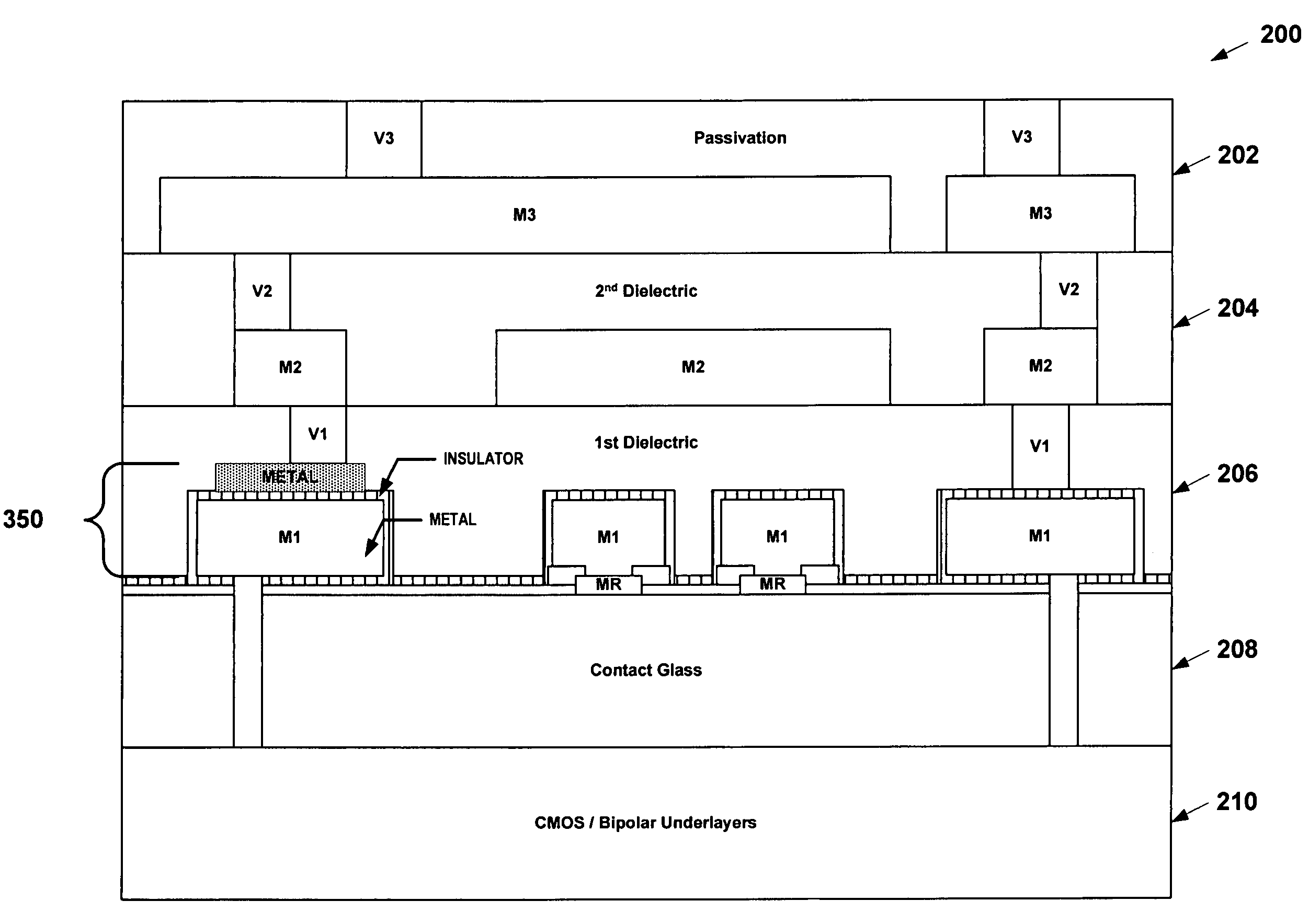
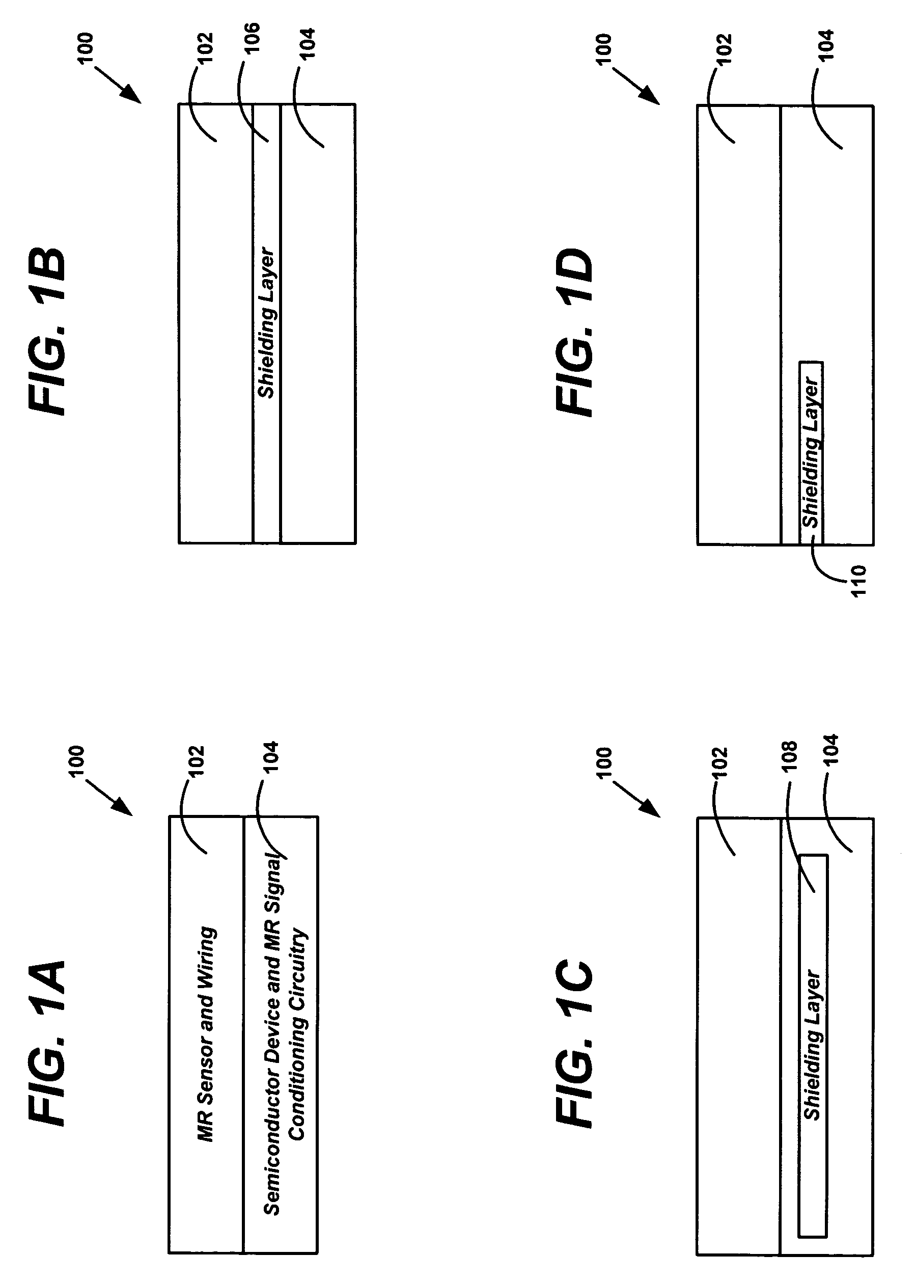
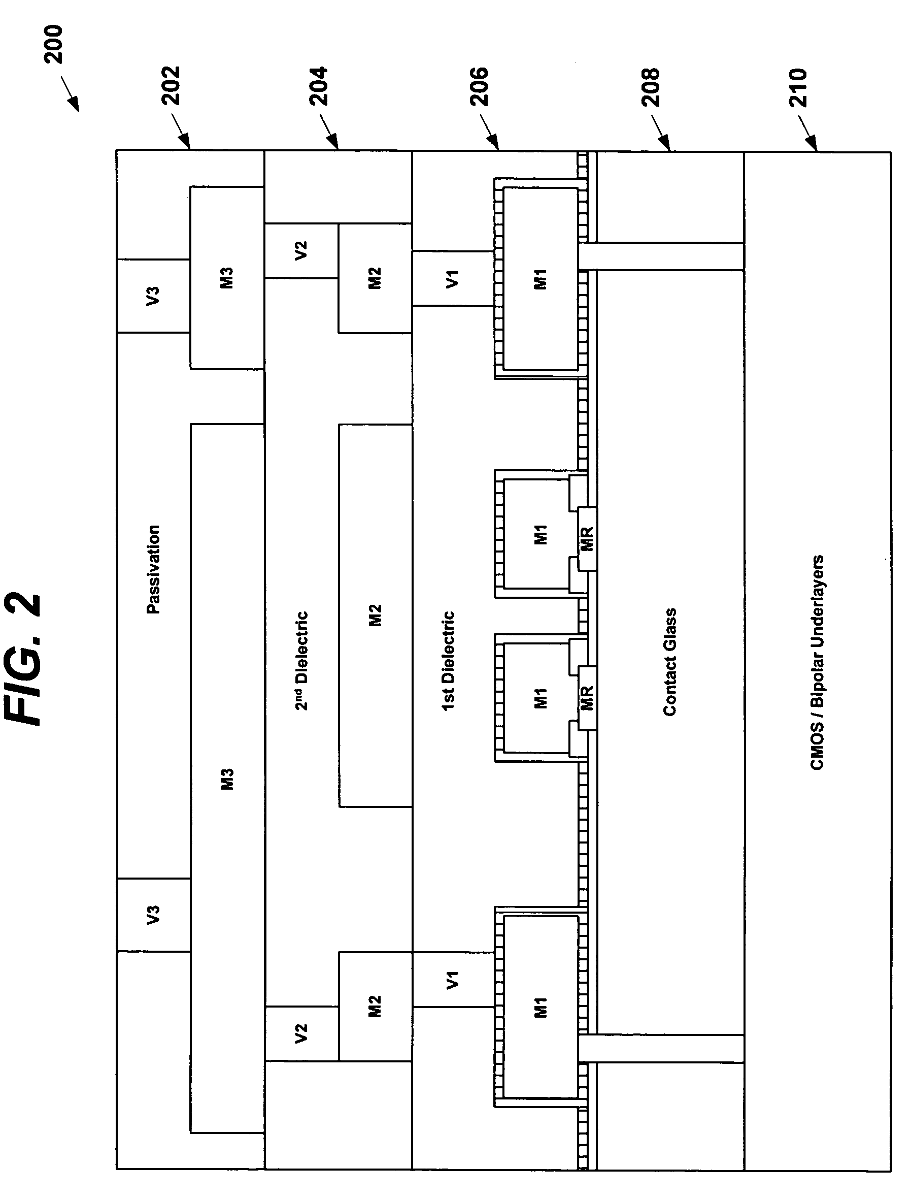
[0022]FIGS. 1A–1B are simplified block diagrams illustrating integration of a semiconductor device with one or more magneto-resistive sensing elements. The device 100 includes a first portion 102, including the magneto-resistive sensing elements (hereinafter collectively referred to as an “MR sensor”) and wiring (such as thin-film traces), and a second portion 104, including one or more semiconductor device components. In a preferred embodiment, the second portion 104 also includes signal conditioning circuitry and circuitry for ESD (Electro-Static Discharge) protection for the MR sensor in the first portion 102. As discussed below, the second portion 104 is particularly amenable to standard semiconducto...


PUM


Abstract

A magnetic-sensing apparatus and method of making and using thereof is provided. The sensing apparatus may be fabricated from semiconductor circuitry and a magneto-resistive sensor. A dielectric may be disposed between the semiconductor circuitry and the magneto-resistive sensor. In one embodiment, the semiconductor circuitry and magneto-resistive sensor are formed into a single package or, alternatively, monolithically formed into a single chip. In another embodiment, some of the semiconductor circuitry may be monolithically formed on a first chip with the magneto-resistive sensor, while other portions of the semiconductor circuitry may be formed on a second chip. As such, the first and second chips may be placed in close proximity and electrically connected together or alternatively have no intentional electrical interaction, Exemplary semiconductor devices that might be implemented include, without limitation, capacitors, inductors, operational amplifiers, set/reset circuitry for the magneto-resistive sensors, accelerometers, pressure sensors, position sensing circuitry, compassing circuitry, etc.

Description

RELATED APPLICATIONS [0001]This application claims the benefit of U.S. Provisional Application Nos. (1) 60 / 475191, filed Jun. 2, 2003, entitled “Semiconductor Device Integration with a Magneto-Resistive Sensor,” naming as inventors Lonny L. Berg and William F. Witcraft; (2) 60 / 475,175, filed Jun. 2, 2003, entitled “On-Die Set / Reset Driver for a Magneto-Resistive Sensor,” naming as inventors Mark D. Amundson and William F. Witcraft; (2) 60 / 475191; and (3) 60 / 462872, filed Apr. 15, 2003, entitled “Integrated GPS Receiver and Magneto-Resistive Sensor Device,” naming as inventors William F. Witcraft, Hong Wan, Cheisan J. Yue, and Tamara K. Bratland. The present application also incorporates each of these Provisional Applications in their entirety by reference herein[0002]This application is also related to and incorporates by reference U.S. Nonprovisional Application Ser. No. 10 / 754945, filed concurrently, entitled “Integrated Set / Reset Driver and Magneto-Resistive Sensor,” naming as in...

Claims


Application Information

Patent Timeline
IPC IPC(8): H01L29/82H01L43/00G01R33/09
CPCG01R33/09G01R33/096
Inventor WITCRAFT, WILLIAM F.BERG, LONNY L.AMUNDSON, MARK D.
Owner HONEYWELL INT INC
Why Eureka
Try Eureka