Method for identifying compounds that affect a transport of a protein through menbrane trafficking pathway

a menbrane trafficking and compound technology, applied in the field of sensors, can solve the problems of limiting the yield of devices, the inability to sequentially develop resistive sensors, and the potential for further miniaturization, and achieves high-quality ohmic contacts, high controllability, and rapid exchange of a few microliters of solution

Inactive Publication Date: 2009-12-03
RGT UNIV OF CALIFORNIA
View PDF1 Cites 21 Cited by
  • Summary
  • Abstract
  • Description
  • Claims
  • Application Information

AI Technical Summary

Benefits of technology

[0019]Thus, the new approach presented in this application can simplify and consolidate the steps of producing 1-D nanomaterials, merging 1-D nanomaterials into lithographically defined electrodes, and integrating electronic and microfluidic components into one. An individually addressable array of conducting polymer nanowires (CPNWs) positioned within an integrated microfluidic device can be electrochemically fabricated in situ. Such an array of CPNWs within an integrated microfluidic device can be used as a chemical sensor immediately after its construction.
[0020]There are certain key advantages to preparing CPNWs within a microfluidic device using spatially localized, template-free electrochemical polymerization: (i) the monomeric precursor polymerizes directly on the electrode surface, producing high-quality ohmic contacts; (ii) addressability is inherent to this method because nanowires can be grown across individual electrode junctions; (iii) the introduction and delivery of small amounts of precursor monomers and analytes is highly controllable and enables the rapid exchange of a few microliters of solution on the chip; (iv) the diffusion-limited transport of the precursor within a microchannel can have a positive effect on the formation of nanowires during the electropolymerization process; and (v) once the nanowires are grown, the entire nanowire / microfluidics circuit is ready for use, without the necessity of any additional processing.

Problems solved by technology

Although many examples have been demonstrated of workable devices and sensors based on 1-D nanostructured materials, it remains a challenge to discover efficient, scalable, and site-specific approaches for incorporating these 1-D nanomaterials into lithographically patterned electrode junctions.
Despite the successes of the above fabrication methods for preparing micro- and nanoscale sensors that incorporate conducting polymer-based nanostructured materials, there are certain limitations in terms of device yields, potential for further miniaturization, scalability, and fabrication costs that prohibit sequential developments of these types of resistive sensors.

Method used


Image

  • Method for identifying compounds that affect a transport of a protein through menbrane trafficking pathway
  • Method for identifying compounds that affect a transport of a protein through menbrane trafficking pathway
  • Method for identifying compounds that affect a transport of a protein through menbrane trafficking pathway

Examples


example 1

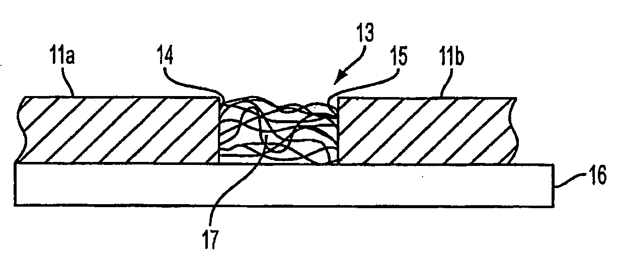
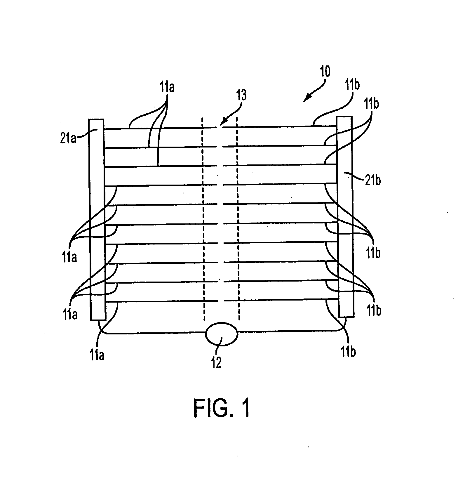
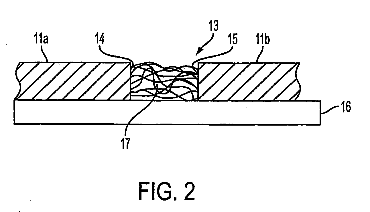
[0036]In this example, we describe the use of electrochemical polymerization, at low and constant current levels, to fabricate, simultaneously and site-specifically, 10 conducting polymer nanoframework electrode junctions (CPNEJs; FIG. 1) in which a number of conducting polymer nanowires (CPNWs) of uniform diameter (for example, from about 40 nm to about 80 nm) intertwine to form nanoframeworks across a 2 μm gap between each pair of platinum (Pt) electrodes without the necessity of using any supporting template. In this example, the CPNWs are polyaniline nanowires. This example demonstrates that the present invention provides a highly efficient electrochemical process for the spontaneous and parallel fabrication of 10 CPNEJs in an array and that the resulting array can be used as a set of resistive junctions to demonstrate real-time electronic sensing in the gas phase and in solution.

[0037]For the fabrication of the CPNEJs, we applied a low-current electrochemical polymerization bas...

example 2

[0048]In this Example, we used the CPNEJ arrays made according to Example 1 as miniaturized resistive sensors for the real-time detection of NH3 (ammonia) and HCl (hydrogen chloride) gases and ethanol vapor. For all measurements in this example, which were performed at room temperature under ambient conditions using a Keithley 4200 semiconductor analyzer, a 0.1 V bias was applied across all of the CPNEJ's in the array and the change in resistance (log(R / R0)), where R is time-dependent resistance and R0 is the initial resistance, was monitored as a function of time. As a first part of this example, we demonstrated the detection of NH3. A CPNEJ array was first doped in 1.0 M aqueous HCl prior to measurement. We measured the real-time change in resistance of an HCl-doped CPNEJ array upon exposure to NH3 (100 ppm) dispersed in an ambient environment. We observed an increase in resistance by 1.2 orders of magnitude within 80 seconds as a result of the de-doping of polyaniline by NH3. Bec...

example 3

[0049]In this example, CPNEJ arrays made according to Example 1 were used to detect a variety of organic vapors, including ethanol, methanol, chloroform and acetone. Initially, we demonstrated the reversible and reproducible response of the CPNEJ array to saturated ethanol vapor. The resistance of the nanoframework increased upon exposure to saturated ethanol vapor, we attribute this increase in resistance to the effect of swelling of the polyaniline backbone caused by the ethanol vapor. The effects of humidity and temperature have noticeable inferences to the absolute conductances (less than 10%) of these CPNEJ array sensors. Although these effects are negligible compared to the analyte-induced conductance changes, they still cause some perturbations in the realistic applications. In order to eliminate these humidity- and temperature-induced perturbations, the real-time responses of these CPNEJ array sensors to gases and vapor were expressed in the form of relative changes (R / R0). ...


PUM

PropertyMeasurementUnit
heightsaaaaaaaaaa
heightsaaaaaaaaaa
heightaaaaaaaaaa

Abstract

Resistive-sensors are provided wherein networks or nanoframeworks of conducting polymer nanowires are electrochemically grown from pre-polymer solutions in the junction gap located between electrode pairs.

Description

BACKGROUND OF THE INVENTION[0001]1. Field of the Invention[0002]The present invention relates generally to sensors that utilize an electrode pair in combination with a sensing element. More particularly, the present invention involves sensors wherein nanostructured materials are used to make up all or part of the sensing element.[0003]2. Description of Related Art[0004]Recent developments in the design and synthesis of conducting one-dimensional (1-D) nanostructured materials, including carbon nanotubes, metal- and / or oxide-based nanowires, and polymer nanowires, have attracted much attention across scientific and engineering disciplines. These 1-D materials have become prime candidates for replacing conventional bulk materials in micro- and nanoelectronic devices and chemical and biological sensors. Although many examples have been demonstrated of workable devices and sensors based on 1-D nanostructured materials, it remains a challenge to discover efficient, scalable, and site-spe...

Claims


Application Information

Patent Timeline
Patent Type & Authority Applications(United States)
IPC IPC(8): G01N27/403B29C41/20
CPCB01J2219/00653B01J2219/00722B01J2219/00731G01N27/127B01L3/5027B82Y15/00G01N27/126B01J2219/00736
Inventor FISCHER, RAINEREMANS, NEILFIORE, STEFANO DIJOCHEMS, CARLOHERRENKNECHT, KURTHURLING, STEPHAN
Owner RGT UNIV OF CALIFORNIA
Why Eureka
Try Eureka