

Electrical memory component and a method of construction thereof
- Summary
- Abstract
- Description
- Claims
- Application Information
AI Technical Summary
Benefits of technology
Problems solved by technology
Method used
Image

Examples
Embodiment Construction
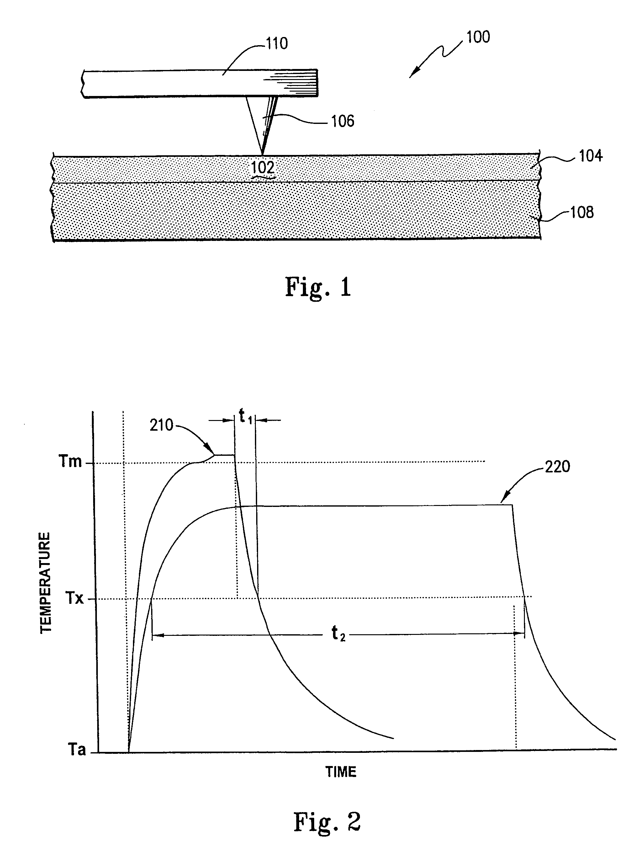
[0011]FIG. 1 is a schematic of a portion of an electrical memory component 100, showing a tip electrode 106 engaging a memory portion 102 of a movable storage media 104. Memory portion 102 includes a portion of storage media 104 subjected to crystallisation and amorphisation during set / reset write operations performed by electrode tip 106. In the exemplary embodiment, storage media 104 includes a film of chalcogenide material, Ge2Sb2Te5, formed over a substrate 108. Many memory portions such as memory portion 102 are provided in two dimensions throughout the storage media 104.
[0012]Tip electrode 106 is mounted on a cantilever arm 110, which is operable to selectively press tip electrode 106 against the storage media 104. Notably, tip electrode 106 tapers to a point, in the exemplary embodiment the point being of the order of 30 nm diameter, and thus provides for a small area of contact to the chalcogenide storage media 104. The small contact is of importance for the resistive phase ...
PUM
 Abstract
Description
Claims
Application Information