Method and apparatus for voltage compensation for parasitic impedance

a parasitic impedance and voltage compensation technology, applied in the field of voltage regulation, can solve the problems of erratic hardware operation, dc-dc conversion, computer hardware is typically voltage intolerant, and the complexity of modern computer hardware is extremely complex and miniaturized

Inactive Publication Date: 2007-07-10
APPLE INC
View PDF11 Cites 21 Cited by
  • Summary
  • Abstract
  • Description
  • Claims
  • Application Information

AI Technical Summary

Benefits of technology

[0014]The voltage regulation circuit may include: a first amplifier having a first input electrically connected to a first node, a second input electrically connected to a third node, and a first output; a second amplifier having a first input electrically connected to a fourth node, a second input electrically connected to a second node, and a second output; an offset generator having a first input electrically connected to the first output from the first amplifier, a second input electrically connected to the second output from the second amplifier, a third input electrically connected to a reference voltage, and an offset output associated with an offset reference voltage and connected to an offset output node; and a compensation amplifier having a first input electrically connected to the first node, and a second input electrically connected to the offset output node. The compensation amplifier operates to drive a voltage at the first node to match the offset reference voltage. This, in turn, permits a voltage across the load to equal the reference voltage by compensating for the voltage loss due to any parasitic impedances.

Problems solved by technology

Computer hardware is typically voltage intolerant.
Changes to the input voltage of 40 or more millivolts may cause erratic operation of the hardware or even hardware failure.
Modern computer hardware is extremely complex and miniaturized.
The dual trends of complexity and miniaturization also render computer hardware more vulnerable to parasitic impedances.
For example, trace or pattern resistances, interference from adjacent hardware, trace or pattern inductance, and dielectric capacitances may all result in a parasitic impedance affecting the operation of a load.
Accordingly, the operation of the load may become unpredictable.
The load may operate erratically or not at all, depending on the impedances and voltage tolerance of the load.
Further, the parasitic impedances may vary with time, thus complicating regulation of voltage to the load.
However, and as shown in FIG. 1, this prior art implementation fails to account for the presence of parasitic impedances 112, 188.
Thus, the prior art voltage regulator 100 may not allow optimal operation (or operation at all) of the load 102.

Method used


Image

  • Method and apparatus for voltage compensation for parasitic impedance
  • Method and apparatus for voltage compensation for parasitic impedance
  • Method and apparatus for voltage compensation for parasitic impedance

Examples


first embodiment

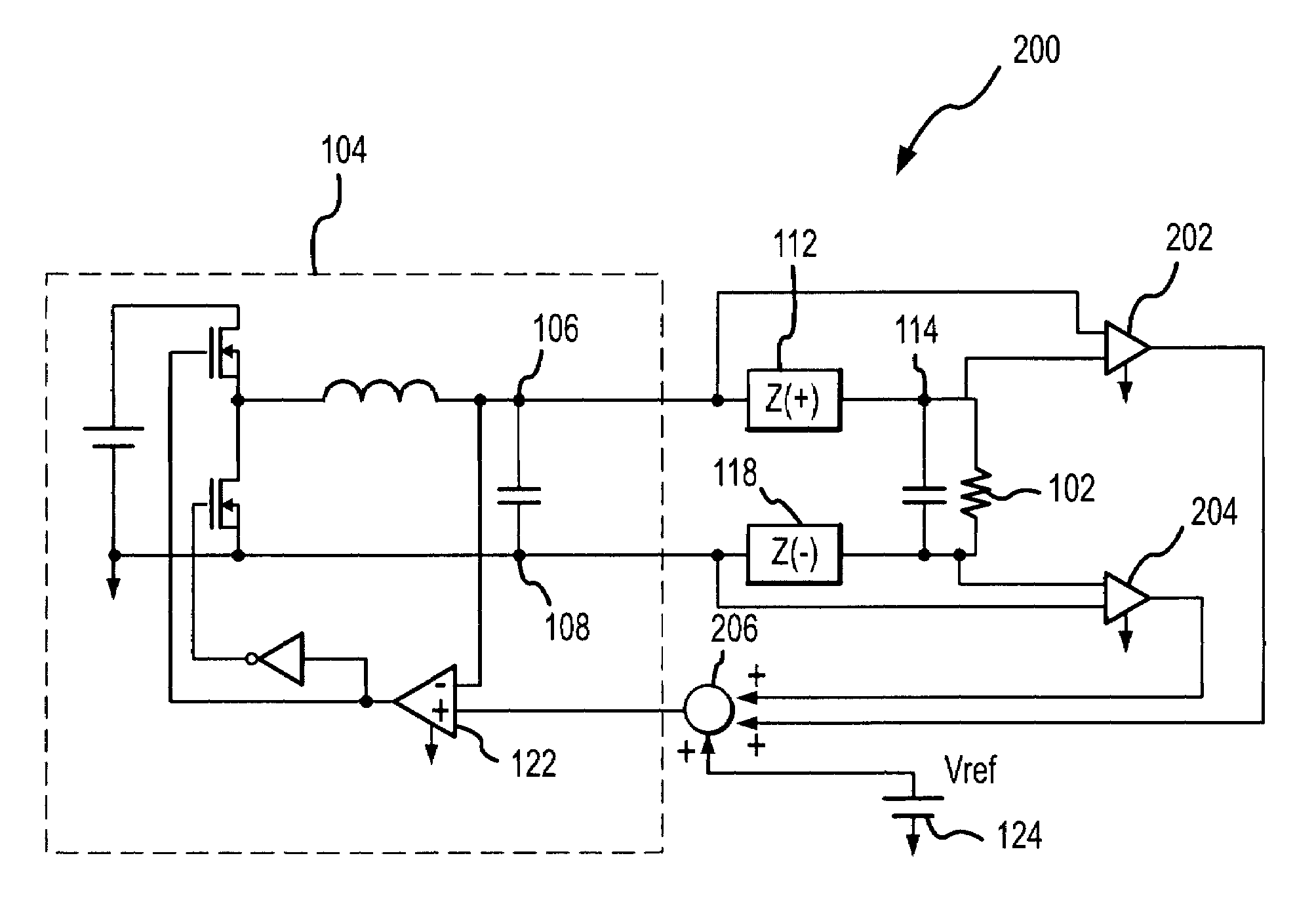
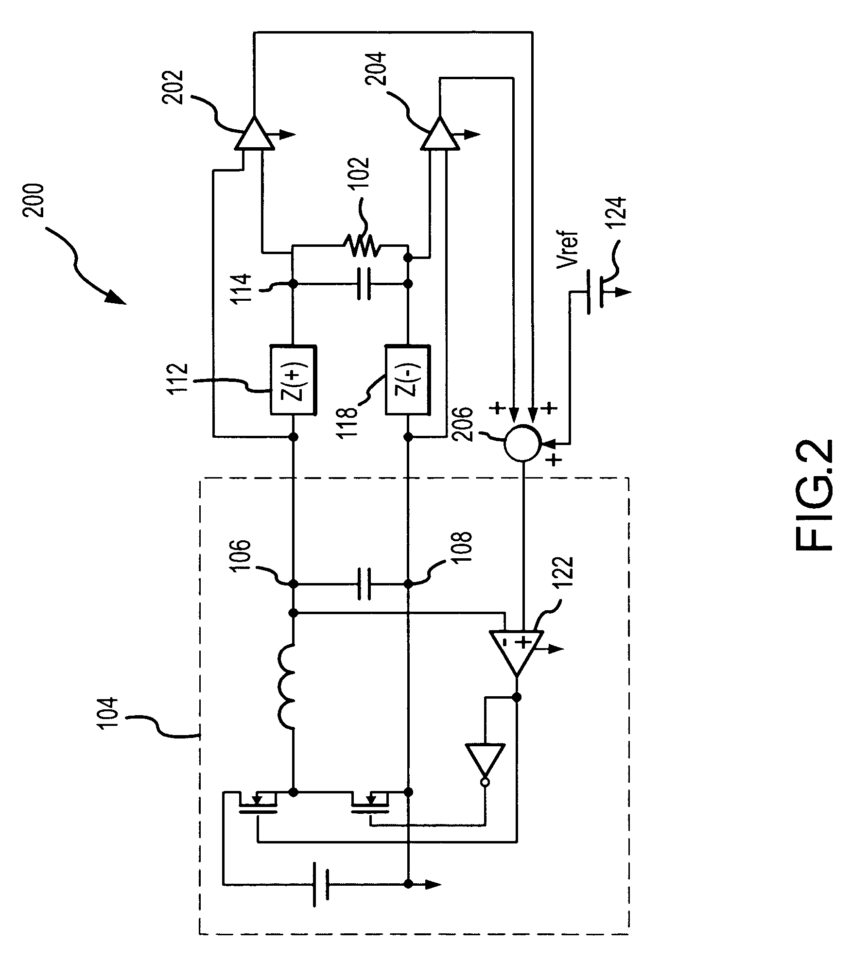
[0034]FIG. 2 depicts a high-level schematic of the invention, namely a voltage regulation circuit 200, affixed to the system or load 102. The present voltage regulation circuit 200 operates to stabilize the input voltage to the load 102 at the desired value.

[0035]The voltage regulation circuit 200 includes a first amplifier 202 and second amplifier 204, each of which produce an input for an offset generator 206. The operation of the amplifiers 202, 204 and generator 206 will be discussed in turn.

[0036]The first amplifier 202 has two inputs. The first input is connected to the first node 106 and the second input to the third node 114. Thus, the voltage difference between the first input and second input of the first amplifier 202 is the voltage drop across the first parasitic impedance 112. Accordingly, the first amplifier 202 outputs a voltage signal equal to this voltage drop.

[0037]Similarly, the second amplifier 204 has a first input connected to the fourth node 116 and a second i...

embodiment 200

[0045]Thus, the voltage at the input of the load 102 is VI+VP2, while the voltage at the load output node 116 is VP2. The load voltage must equal the difference between input and output voltages, which is the desired input voltage VI. In this manner, the present embodiment 200 may supply a load 102 with a voltage equal to a desired input voltage (or at least within a desired voltage tolerance of the input voltage), regardless of any parasitic impedances experienced by the system.

[0046]FIG. 3 depicts a more detailed schematic of the embodiment of FIG. 2. Specifically, FIG. 3 depicts the circuitry employed to construct the first amplifier 202, second amplifier 204, and offset generator 206. The first amplifier 202, for example, consists of a first resistor 210 electrically connected to the first node 106 and a first amplifier node 227, a second resistor 212 electrically tied to the first amplifier node 227 and a second amplifier node 230, a third amplifier resistor 214 in electrical c...


PUM


Abstract

An apparatus and method for regulating a voltage to a load to compensate for one or more parasitic impedances. A first amplifier measures the voltage drop due to a first parasitic impedance, and a second amplifier measures the voltage drop due to a second parasitic impedance. An offset generator sums the first and second voltage drops with a reference voltage, and drives a DC-to-DC converter to produce an input voltage matching the summed voltages. Accordingly, the voltage at a load between the parasitic impedances matches the reference voltage. The load may be, for example, a computer microprocessor or central processing unit.

Description

BACKGROUND OF THE INVENTION[0001]1. Technical Field[0002]The present invention relates generally to a method and apparatus for voltage regulation, and more specifically to methods and apparatuses for regulating voltage in computer hardware to compensate for one or more parasitic impedances.[0003]2. Background Art[0004]Many electronics systems employ a DC-to-DC converter to change one voltage to another. Typically, the DC-to-DC converter acts on a supply voltage to produce an input voltage. The input voltage and supply voltages are both direct current (DC) voltages. For example, many computing applications employ a DC-to-DC converter to step down a high supply voltage to a desired input voltage, which is then used to power a microprocessor such as a central processing unit (CPU), microprocessing unit (MPU), application-specific integrated circuit (ASIC), and so forth (collectively, a “load”).[0005]Computer hardware is typically voltage intolerant. That is, computer hardware requires ...

Claims


Application Information

Patent Timeline
Patent Type & Authority Patents(United States)
IPC IPC(8): G05F1/00
CPCH02M3/157H02M3/1588Y02B70/1466Y02B70/10
Inventor KANAMORI, TAKASHIKIM, STEPHEN J.JAUREGUI, DAVID
Owner APPLE INC
Why Eureka
Try Eureka