Semiconductor module mounting structure, a cardlike semiconductor module, and heat receiving members bonded to the cardlike semiconductor module

a semiconductor module and mounting structure technology, applied in semiconductor/solid-state device details, cooling/ventilation/heating modification, semiconductor devices, etc., can solve problems such as adverse invasion, thermal expansion and contraction, and undesirable air layers, and achieve the effect of reducing the thickness of sealing resin

Active Publication Date: 2007-07-10
DENSO CORP
View PDF42 Cites 22 Cited by
  • Summary
  • Abstract
  • Description
  • Claims
  • Application Information

AI Technical Summary

Benefits of technology

[0013]More specifically, the present invention has an object to provide a semiconductor module mounting structure capable of adequately preventing external air from entering into grease gaps between the metallic radiator plates and the heat receiving members regardless of repetitive expansions and contractions of the semiconductor module.
[0016]In order to accomplish the above and other related objects, the present invention provides a cardlike semiconductor module including a semiconductor chip, a sealing resin accommodating the semiconductor chip and having two principal surfaces substantially parallel to each other, and metallic radiator plates having flat heat dissipating surfaces exposed from the principal surfaces of the sealing resin and fixed on central regions of the principal surfaces of the sealing resin. The principal surfaces of the sealing resin define grease reservoirs surrounding the metallic radiator plates. And, the grease reservoirs are arranged by reducing the thickness of the sealing resin at principal surfaces corresponding to the grease reservoirs compared with the thickness of the sealing resin at principal surfaces corresponding to the metallic radiator plates.

Problems solved by technology

However, the repetitive expansions and contractions in the thickness direction will cause problems.
However, strictly speaking, the heat receiving members themselves cause thermal expansions and contractions.
Such repetitive shifting of the grease in the surface direction will induce adverse invasion of external air into respective grease gaps and will leave undesirable air layers between the heat receiving members and the metallic radiator plates.
However, according to ordinary cardlike semiconductor module stack structures, flexibly changing the distance between the paired heat receiving members in accordance with expansions and contractions of the cardlike semiconductor module is very difficult because these heat receiving members are fixed in a casing or housing in many cases.
However, in view of strength of the cardlike semiconductor module, it is difficult to give the power semiconductor module a sufficient capability of elastically compressing.

Method used


Image

  • Semiconductor module mounting structure, a cardlike semiconductor module, and heat receiving members bonded to the cardlike semiconductor module
  • Semiconductor module mounting structure, a cardlike semiconductor module, and heat receiving members bonded to the cardlike semiconductor module
  • Semiconductor module mounting structure, a cardlike semiconductor module, and heat receiving members bonded to the cardlike semiconductor module

Examples


first embodiment

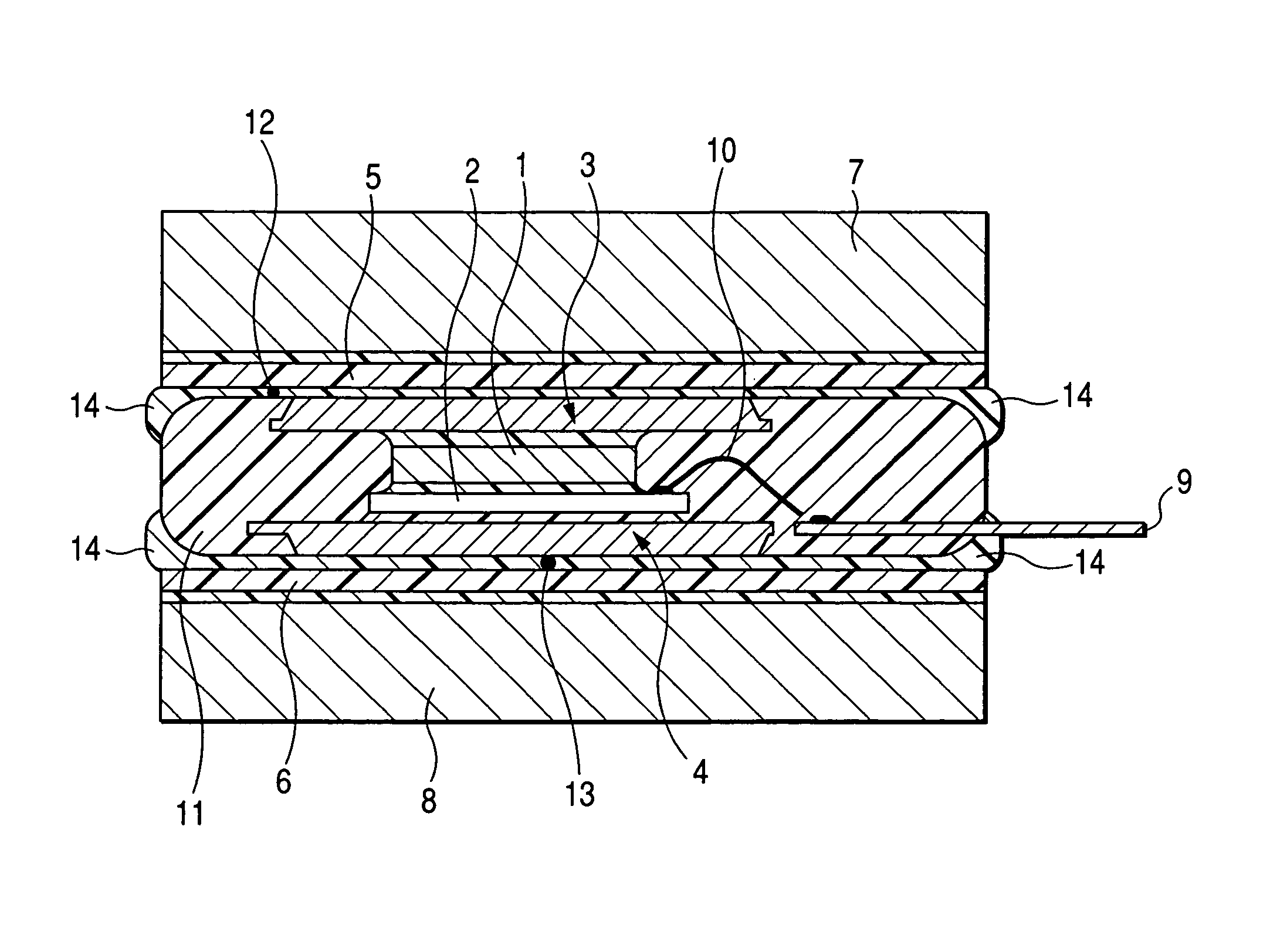
[0065]A semiconductor module mounting structure in accordance with a first embodiment of the present invention will be explained with reference to FIG. 1. FIG. 1 is a cross-sectional side view showing a semiconductor module mounting structure in accordance with the first embodiment of the present invention.

[0066]A semiconductor module used in this semiconductor module mounting structure is a thin-plate cardlike semiconductor module (hereinafter, referred to as a semiconductor module) which accommodates a semiconductor chip 2. The semiconductor chip 2 has an upper principal surface on which a first principal electrode (not shown) is formed. The first principal electrode is bonded, for example by solder joint, to a metallic member 1 having excellent electric conductivity. The metallic member 1 has a front end portion (not shown) extending to the outside so as to form a first principal electrode terminal. Furthermore, the metallic member 1 has an upper surface bonded, for example by so...

second embodiment

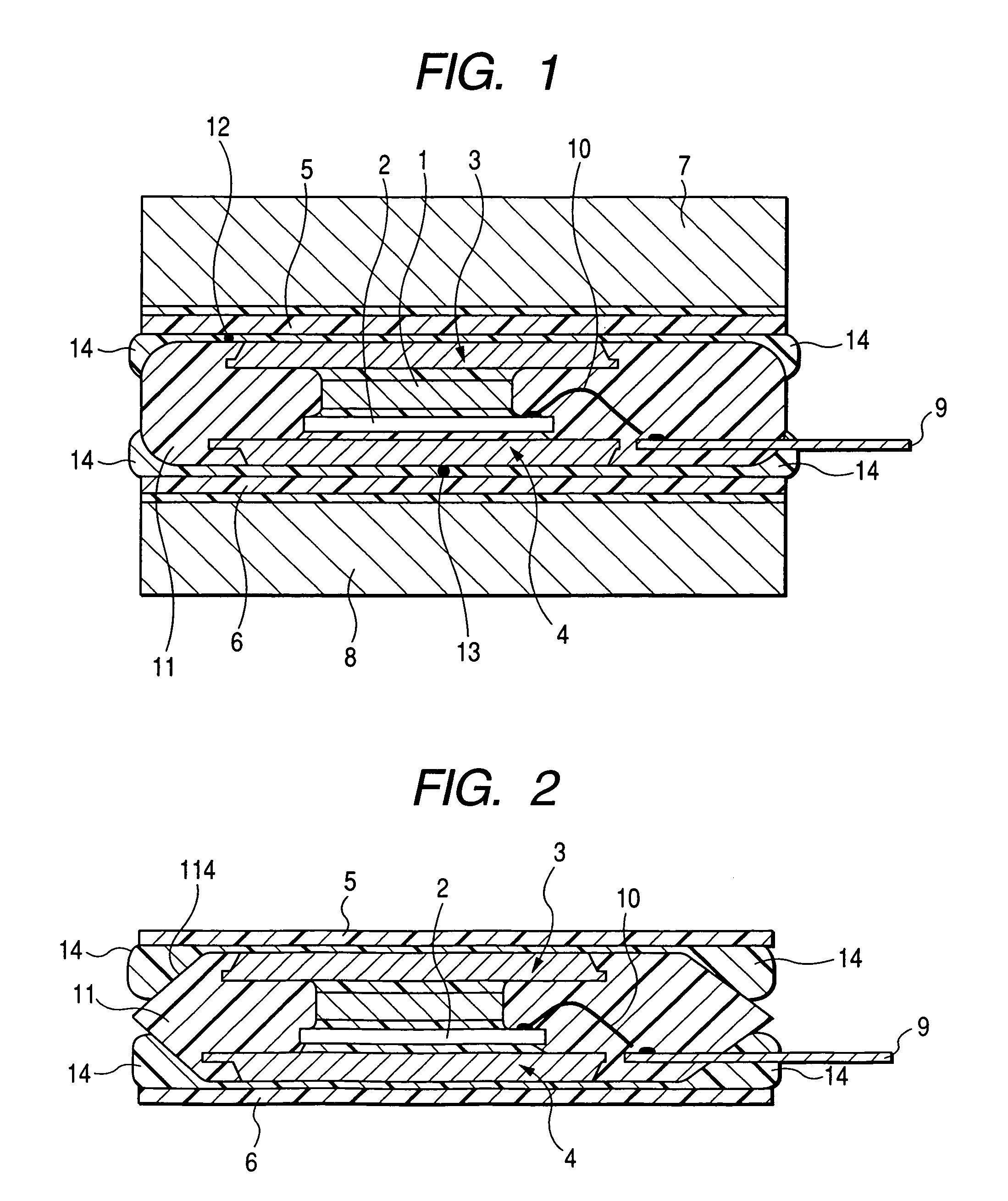
[0075]A semiconductor module mounting structure in accordance with a second embodiment of the present invention will be explained hereinafter with reference to FIG. 2. This embodiment is characterized in that tapered surfaces 114 are provided on the principal surfaces of the sealing resin 11 instead of forming the round chamfered portions at the peripheral corner portions of the sealing resin 11 as disclosed in the first embodiment. The tapered surfaces 114, i.e. inclined flat surfaces, define the grease reservoirs 14 surrounding the metallic radiator plates 3 and 4. This embodiment brings the effects substantially similar to those brought by the first embodiment.

third embodiment

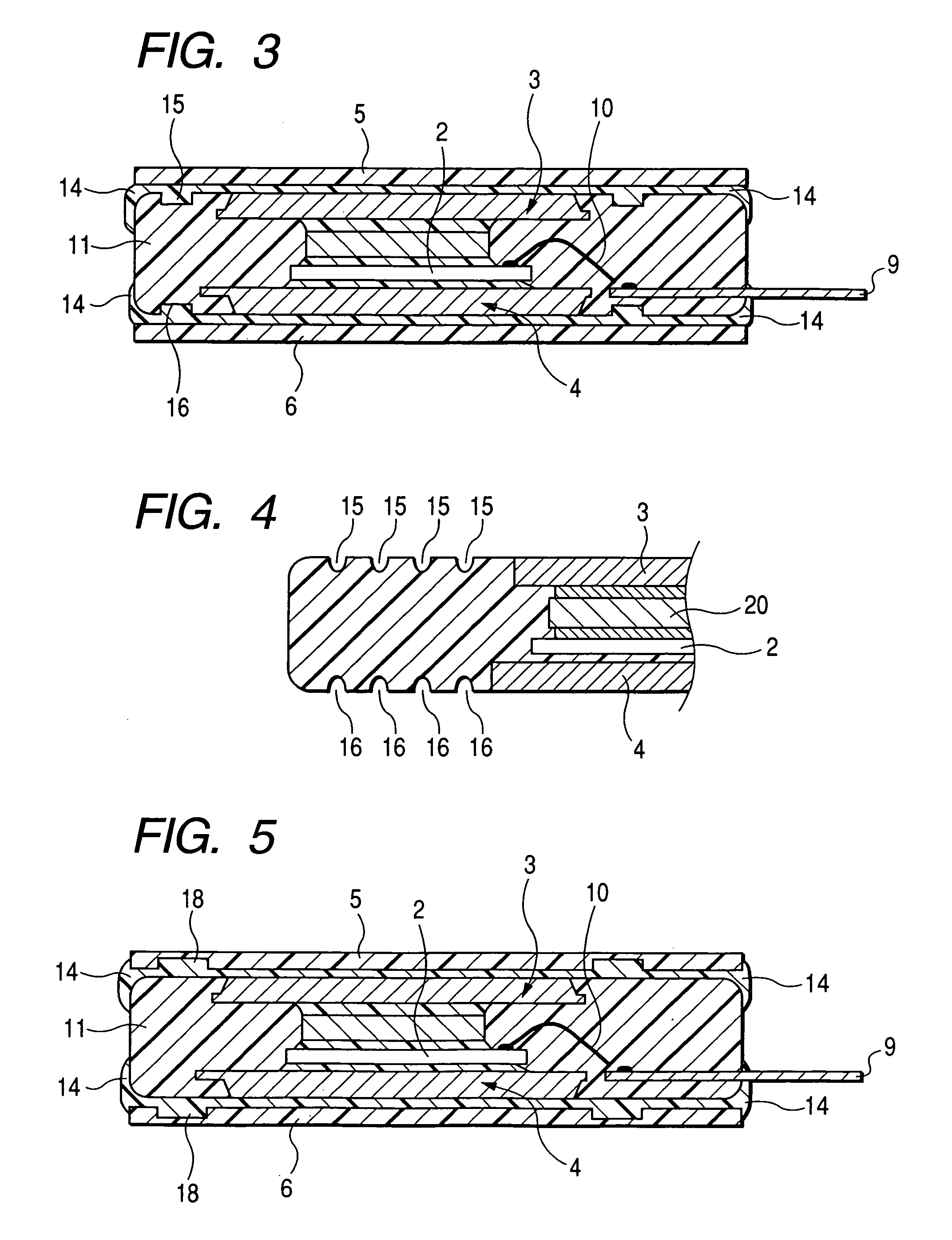
[0076]A semiconductor module mounting structure in accordance with a third embodiment of the present invention will be explained hereinafter with reference to FIG. 3. This embodiment is characterized in that grooves 15 and 16 are provided on the principal surfaces of the sealing resin 11 along the periphery of the sealing resin 11 so as to surround the metallic radiator plates 3 and 4. This embodiment brings the effects substantially similar to those brought by the first embodiment. To ensure the effects of the present invention, it is preferable to provide the grooves 15 and 16 so as to extend entirely along the periphery of the metallic radiator plates 3 and 4.


PUM


Abstract

A semiconductor module has metallic radiator plates provided at central regions of principal surfaces of a sealing resin so as to expose from these principal surfaces. The metallic radiator plates and the principal surfaces of the sealing resin are bonded via grease gaps to heat receiving members. The grease gaps are widened in outer regions far from the metallic radiator plates compared with inner regions adjacent to the metallic radiator plates, to prevent external air from entering into the grease gaps even when the semiconductor module causes repetitive thermal expansions and contractions.

Description

CROSS-REFERENCE TO RELATED APPLICATION[0001]This application is based upon and claims the benefit of priority from earlier Japanese Patent Application No. 2004-124663 filed on Apr. 20, 2004 so that the description of which is incorporated herein by reference.BACKGROUND OF THE INVENTION[0002]The present invention relates to a semiconductor module mounting structure, a cardlike semiconductor module, and heat receiving members bonded to the cardlike semiconductor module. The present invention is preferably applicable to a semiconductor module mounting structure for bonding a cardlike semiconductor module (i.e. a so-called double-sided semiconductor module having electrodes on both surfaces thereof) to the members to be bonded with thermal conductive grease.[0003]To improve heat radiation properties of a power semiconductor module incorporating a semiconductor switching element chip used for electric power control, the Japanese patent application Laid-open No. 2000-243881 discloses a ca...

Claims


Application Information

Patent Timeline
Patent Type & Authority Patents(United States)
IPC IPC(8): H05K7/20H01L23/34H01L23/31H01L23/42H01L23/433
CPCH01L23/3107H01L23/42H01L23/4334H01L24/32H01L24/33H01L2224/32014H01L2224/48091H01L2224/48247H01L2224/73215H01L2224/73265H01L2924/01013H01L2924/01029H01L2924/01047H01L2924/1815H01L2924/18301H01L2924/00014H01L24/48H01L2224/32245H01L2924/01006H01L2924/01033H01L2924/00H01L2224/2612H01L2224/48464H01L2224/83951H01L2224/8592H01L2924/14H01L2924/181H01L2924/00012H01L2224/45099H01L2224/45015H01L2924/207
Inventor KURAUCHI, TSUYOSHINAKANO, TOMOAKIARAI, HIROAKI
Owner DENSO CORP
Why Eureka
Try Eureka