Method for manufacturing solid-state imaging devices

a solid-state imaging and manufacturing method technology, applied in the field of manufacturing solid-state imaging devices, can solve the problems of increasing manufacturing costs, affecting the quality of solid-state imaging devices, so as to avoid deformation of the housing, reduce manufacturing costs, and reduce manufacturing costs

Active Publication Date: 2007-07-24
PANASONIC SEMICON SOLUTIONS CO LTD
View PDF51 Cites 24 Cited by
  • Summary
  • Abstract
  • Description
  • Claims
  • Application Information

AI Technical Summary

Benefits of technology

[0008]It is an object of the present invention to provide a method for manufacturing a solid-state imaging device, in which it is possible to make a low cost housing with minimal deformation, avoiding deformation of the housing caused by a difference in thermal expansion between a wiring board and a rib made of a resin during batch manufacture of the housing for the purpose of configuring a plurality of solid-state imaging devices.
[0009]It is another object of the present invention to provide a method for manufacturing a solid-state imaging device with which it is possible to provide a rib with a reverse taper by a simple process.

Problems solved by technology

The casting mold for molding the housing with resin is matched to the housing specification and must be made for each product, leading to an increase in the manufacturing cost.
However, when molding resin ribs onto the wiring board, deformations of the housing such as warping and twisting tend to occur, caused by the difference in thermal expansion between the wiring board containing metal wires and the rib made of a resin.
This problem is particularly conspicuous when manufacturing a plurality of housings for solid-state imaging devices all together.
However when the taper direction is provided such that the rib width increases away from the board surface (called a “reverse taper” below), an impediment to rib resin molding develops.
That is to say, if the housing structure is formed integrally with the rib 28 on the upper surface of the peripheral portion of the base 21, or if the rib is resin-molded onto the wiring board, mold release after molding of the portion of the forming die which forms the internal space of the housing becomes problematic because of the rib's reverse taper.

Method used


Image

  • Method for manufacturing solid-state imaging devices
  • Method for manufacturing solid-state imaging devices
  • Method for manufacturing solid-state imaging devices

Examples


Embodiment Construction

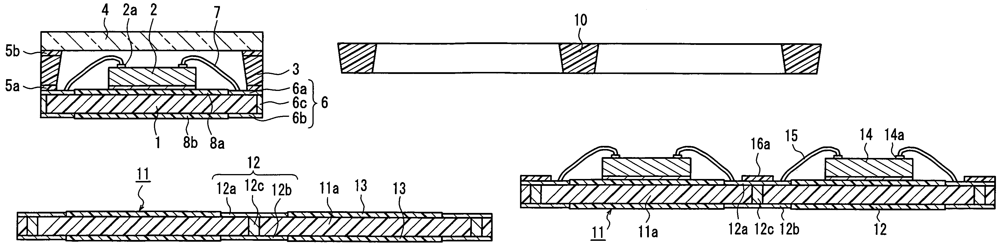
[0019]According to the method for manufacturing solid-state imaging devices in the present invention, a separate resin formed rib forming member is joined to a wiring board, thus avoiding deformation of the housing caused by a difference in thermal expansion between the wiring board and the resin ribs at the time of resin molding, and it is possible to manufacture a low cost housing with high accuracy.

[0020]Furthermore, because the rib forming member is independently resin molded, there is no obstruction to mold release after resin molding of the taper formed on the rib.

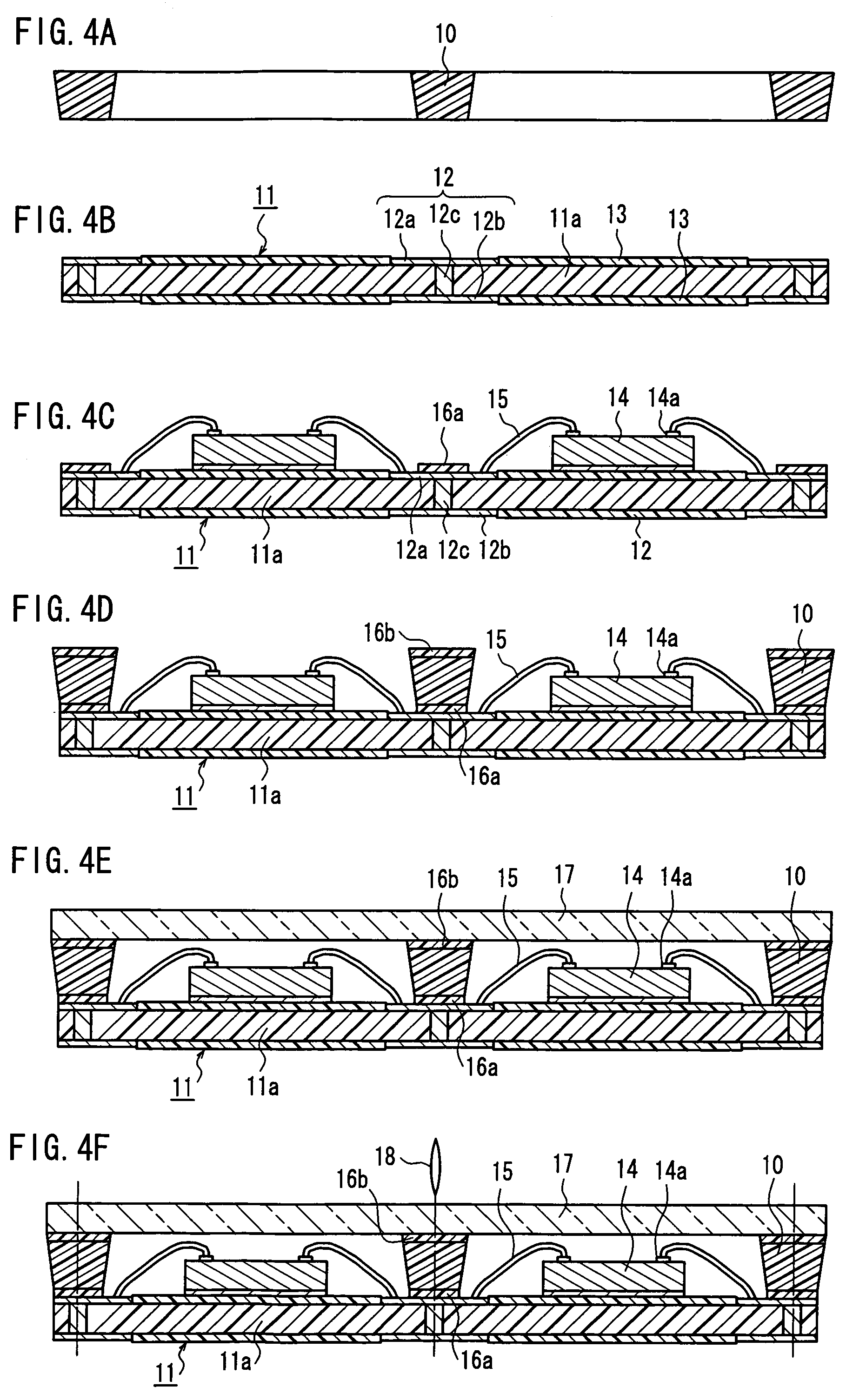
[0021]In the method for manufacturing solid-state imaging devices according to the present invention, it is possible that, when fastening the transparent plate, the transparent plate of a size covering the plurality of housings is fastened to the top face of the rib forming member, and when cutting each housing, the transparent plate also is cut at the same time. Alternatively, when fastening the transparent plate, a...


PUM


Abstract

A solid-state imaging device is manufactured according to the steps below. A lattice-shaped rib forming member, which is an aggregation of a plurality of frame-shaped ribs for configuring a plurality of solid-state imaging devices, is resin-molded. An aggregate wiring board is used, which has regions corresponding to a plurality of the wiring boards, and in which a plurality of the wiring members are provided in each of the regions, and the imaging element is fastened to each region of the aggregate wiring board and the electrodes of the imaging elements and the wiring members are connected by a thin metal wire. The rib forming member is placed on the wiring board face and joined to the wiring board face, so that the imaging element is disposed inside the lattice elements of the rib forming member. The transparent plate is fastened to an upper face of the rib forming member, and each housing is cut in a direction perpendicular to the base portion, and in a direction dividing into two the width of the rib forming member, and separating the solid-state imaging devices into individual pieces It is possible to make a low cost housing, avoiding deformations caused by a difference in thermal expansion between the wiring board and the ribs made of a resin, when forming a plurality of housings together.

Description

FIELD OF THE INVENTION[0001]The present invention relates to methods for manufacturing solid-state imaging devices in which imaging elements such as CCDs or the like are mounted within a housing.BACKGROUND OF THE INVENTION[0002]Solid state imaging devices, which are widely used for video cameras and still cameras and the like, are provided in the form of a package, in which an imaging element such as a CCD or the like is mounted on a base made of an insulating material, with the photodetecting region being covered by a transparent plate. In order to make the device more compact, the imaging element is mounted as a bare chip on the base. Referring to FIG. 7, the following is an explanation of the solid-state imaging device disclosed in JP H5-267629A as a conventional example of these types of solid-state imaging devices.[0003]In FIG. 7, numeral 21 denotes a base, on the top face of which is formed a recess portion. An imaging element chip 22 is formed in the center of the recess port...

Claims


Application Information

Patent Timeline
Patent Type & Authority Patents(United States)
IPC IPC(8): H01L21/00H01L21/50H01L27/14H01L23/00H01L23/02H01L23/34H01L23/50H01L27/146H01L31/0203H04N5/335H04N101/00
CPCH01L24/97H01L27/14618H01L27/14625H01L27/14683H01L2224/32225H01L2224/48091H01L2224/48227H01L2224/73265H01L2224/97H01L2924/01033H01L2924/01078H01L2924/01082H01L2924/15153H01L2924/15165H01L2924/16195H01L2924/00014H01L2224/83H01L2224/85H01L2924/01005H01L2924/01006H01L2924/00H01L2924/00012H01L2924/181H01L24/73H01L27/146H01L23/00
Inventor YAMAUCHI, KOUICHIMINAMIO, MASANORISHIMIZU, KATSUTOSHINAGATA, HARUTO
Owner PANASONIC SEMICON SOLUTIONS CO LTD
Why Eureka
Try Eureka