
III-nitride material structures including silicon substrates

a gallium nitride and substrate technology, applied in the field of iiinitride materials, can solve the problems of limited commercialization of structures and devices that include gallium nitride materials formed on silicon substrates, cracks and/or other types of defects in gallium nitride material layers, and the difference between iii-nitride materials and many substrate materials,

Inactive Publication Date: 2007-07-24
MACOM TECH SOLUTIONS HLDG INC
View PDF78 Cites 86 Cited by
  • Summary
  • Abstract
  • Description
  • Claims
  • Application Information

AI Technical Summary

Problems solved by technology

However, property differences between III-nitride materials (e.g., gallium nitride materials) and many substrate materials can present challenges.
These differences may lead to formation of cracks and / or other types of defects in gallium nitride material layers that are grown on silicon.
However, these differences (and others) have limited commercialization of structures and devices that include gallium nitride material formed on silicon substrates.
When energy is dissipated in high frequency devices through undesirable mechanisms, the performance of the device may be impaired.
These so-called parasitic losses can reduce output power, power gain and efficiency.

Method used


Image

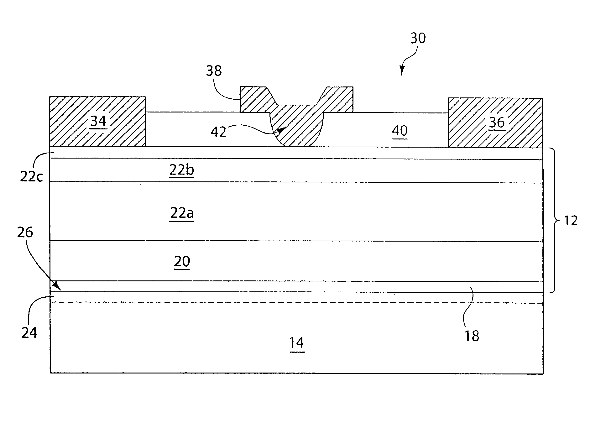
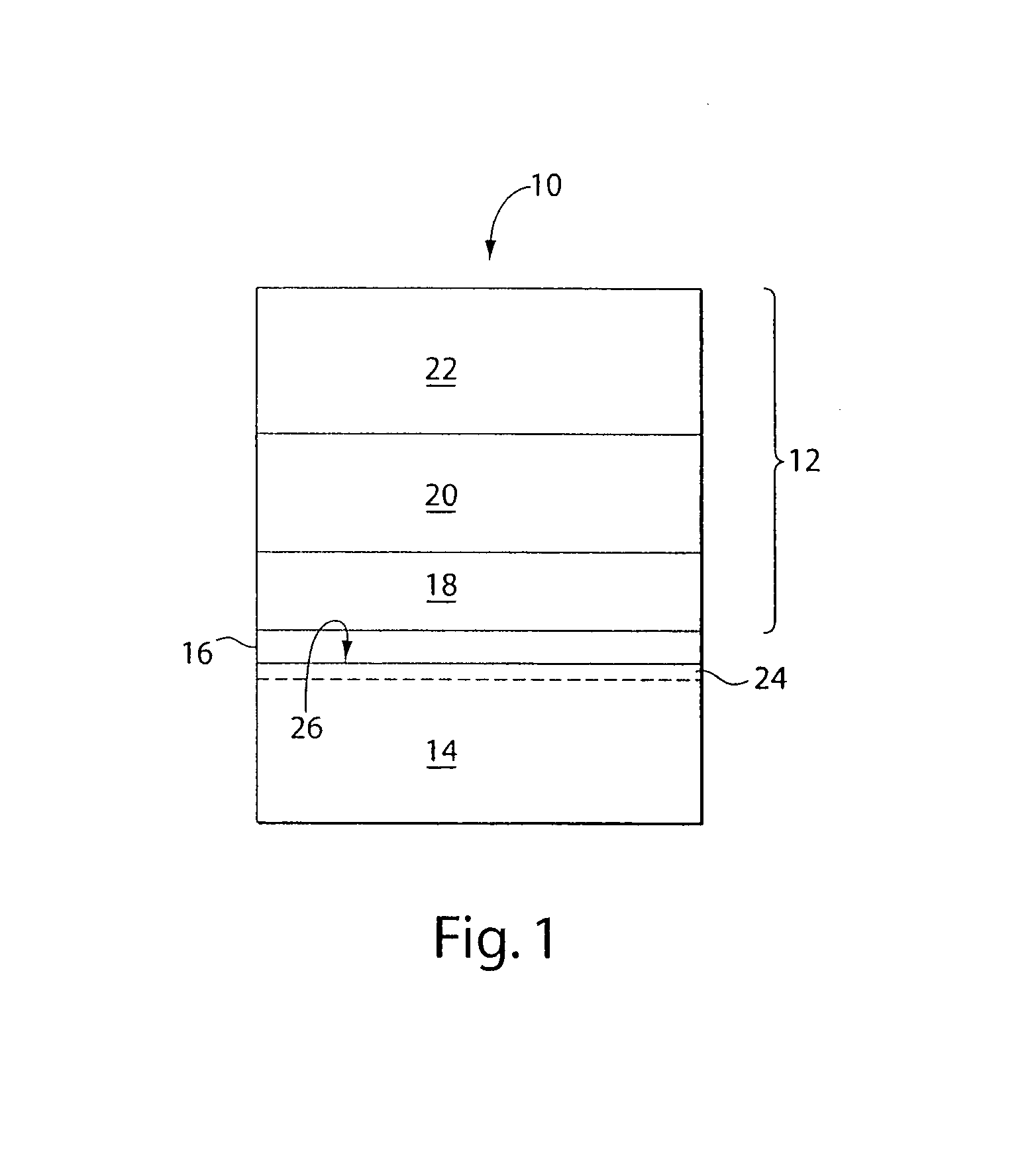
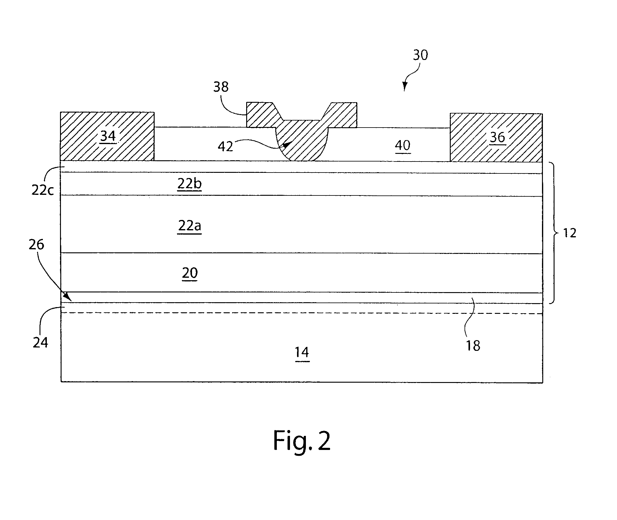
  • III-nitride material structures including silicon substrates
  • III-nitride material structures including silicon substrates
  • III-nitride material structures including silicon substrates

Examples


example 1

[0093]This example compares a structure produced according to a method of the invention that includes a parasitic channel having a reduced free carrier concentration to a structure produced according to a conventional method in which the free carrier concentration of the parasitic channel is not reduced.

[0094]Both methods started with a 100 mm silicon substrate (111) having a resistivity of greater than about 104 ohm-cm. Both methods involved growing an AlN layer on the substrates in a MOCVD reactor at a nominal growth temperature of about 1030° C.

[0095]In the conventional method, the aluminum source gas was introduced into the reactor chamber followed by introduction of the nitrogen source gas.

[0096]In the method of the invention, the nitrogen source gas was introduced into the reactor chamber prior to the introduction of the aluminum source. This is believed to form a silicon nitride layer directly on the surface of the substrate which, as noted in the description above, can funct...

example 2

[0100]This example compares structures produced according to a method of the invention to a structure produced according to a conventional method.

[0101]Both methods started with a 100 mm silicon substrate (111) having a resistivity of greater than about 104 ohm-cm. Both methods involved growth processes in an MOCVD reactor at a nominal growth temperature of about 1030° C. In both cases, an AlN intermediate layer was grown on the silicon substrate; a compositionally-graded AlGaN transition layer was grown on the intermediate layer; a GaN layer was grown on the transition layer; and, an AlGaN layer was grown on the GaN layer.

[0102]In the conventional method, the aluminum source gas was introduced into the reactor chamber followed by introduction of the nitrogen source gas at the start of the growth process.

[0103]In the methods of the invention, the nitrogen source gas was introduced into the reactor chamber prior to the introduction of the aluminum source. This is believed to form a s...


PUM


Abstract

III-nitride material structures including silicon substrates, as well as methods associated with the same, are described. Parasitic losses in the structures may be significantly reduced which is reflected in performance improvements. Devices (such as RF devices) formed of structures of the invention may have higher output power, power gain and efficiency, amongst other advantages.

Description

FIELD OF INVENTION[0001]The invention relates generally to III-nitride materials and, more particularly, to gallium nitride material structures including silicon substrates.BACKGROUND OF INVENTION[0002]III-nitride materials include gallium nitride (GaN), aluminum nitride (AlN), indium nitride (InN) and their respective alloys (e.g., AlGaN, InGaN, AlInGaN and AlInN). In particular, gallium nitride materials include gallium nitride (GaN) and its alloys such as aluminum gallium nitride (AlGaN), indium gallium nitride (InGaN), and aluminum indium gallium nitride (AlInGaN). These materials are semiconductor compounds that have a relatively wide, direct bandgap which permits highly energetic electronic transitions to occur. Such electronic transitions can result in gallium nitride materials having a number of attractive properties including the ability to efficiently emit blue light, the ability to transmit signals at high frequency, and others.[0003]In many applications, III-nitride mate...

Claims


Application Information

Patent Timeline
Patent Type & Authority Patents(United States)
IPC IPC(8): H01L31/00H01L21/28
CPCH01L29/2003H01L29/267H01L29/7787
Inventor HANSON, ALLEN W.ROBERTS, JOHN CLAASSENPINER, EDWIN L.RAJAGOPAL, PRADEEP
Owner MACOM TECH SOLUTIONS HLDG INC
Learn More