Semiconductor memory device having controller with improved current consumption

a memory device and semiconductor technology, applied in the field of semiconductor memory devices, can solve the problems of large power consumption

Inactive Publication Date: 2007-07-24
SK HYNIX INC
View PDF12 Cites 35 Cited by
  • Summary
  • Abstract
  • Description
  • Claims
  • Application Information

AI Technical Summary

Benefits of technology

[0010]Accordingly, the present invention has been made in view of the above problems, and it is an object of the present invention to provide a semiconductor memory device in which the current consumed in a column address counter at the time of a read operation can be reduced.

Problems solved by technology

Thus, lots of power is consumed.

Method used


Image

  • Semiconductor memory device having controller with improved current consumption
  • Semiconductor memory device having controller with improved current consumption
  • Semiconductor memory device having controller with improved current consumption

Examples


Embodiment Construction

[0019]Now, the preferred embodiments according to the present invention will be described with reference to the accompanying drawings.

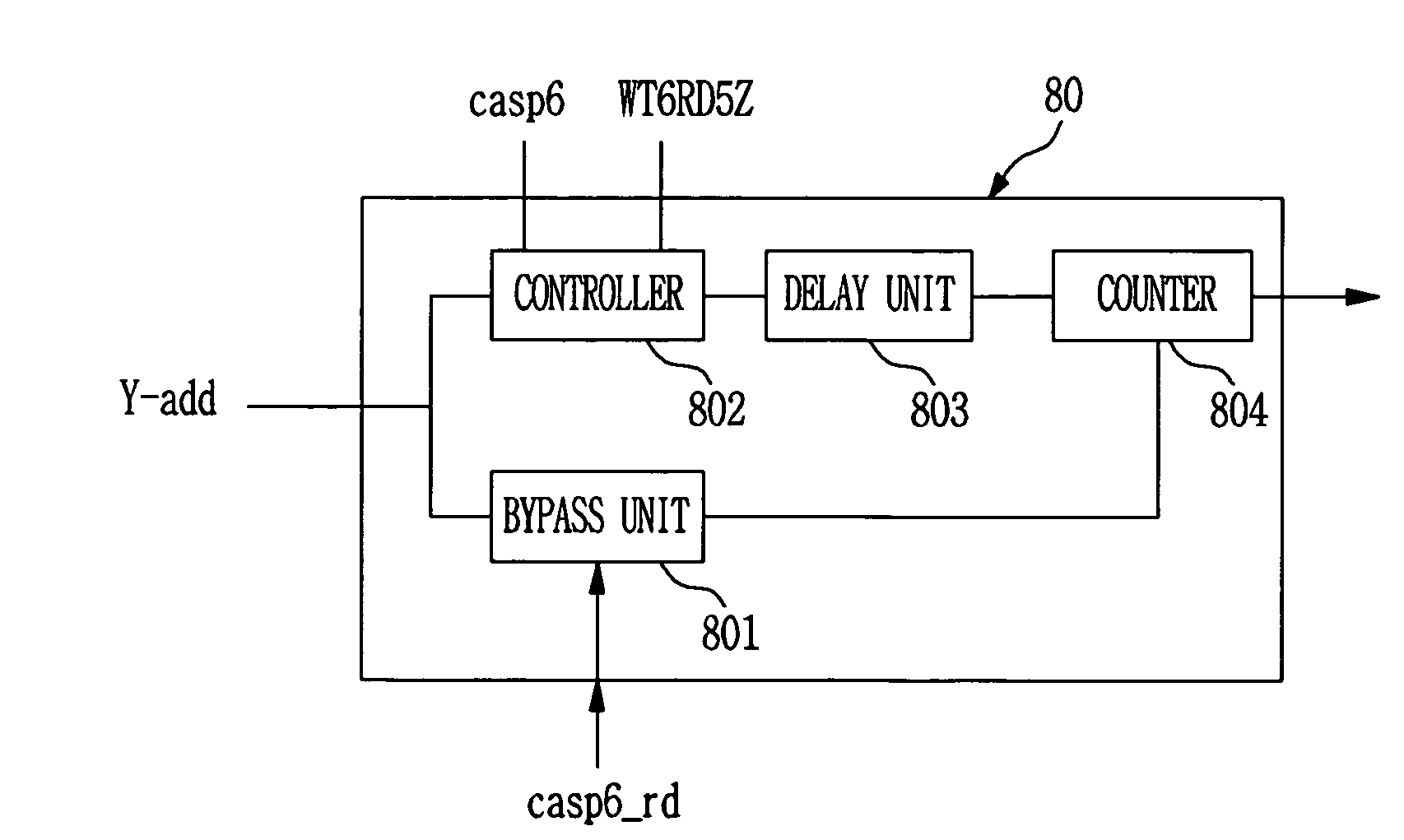
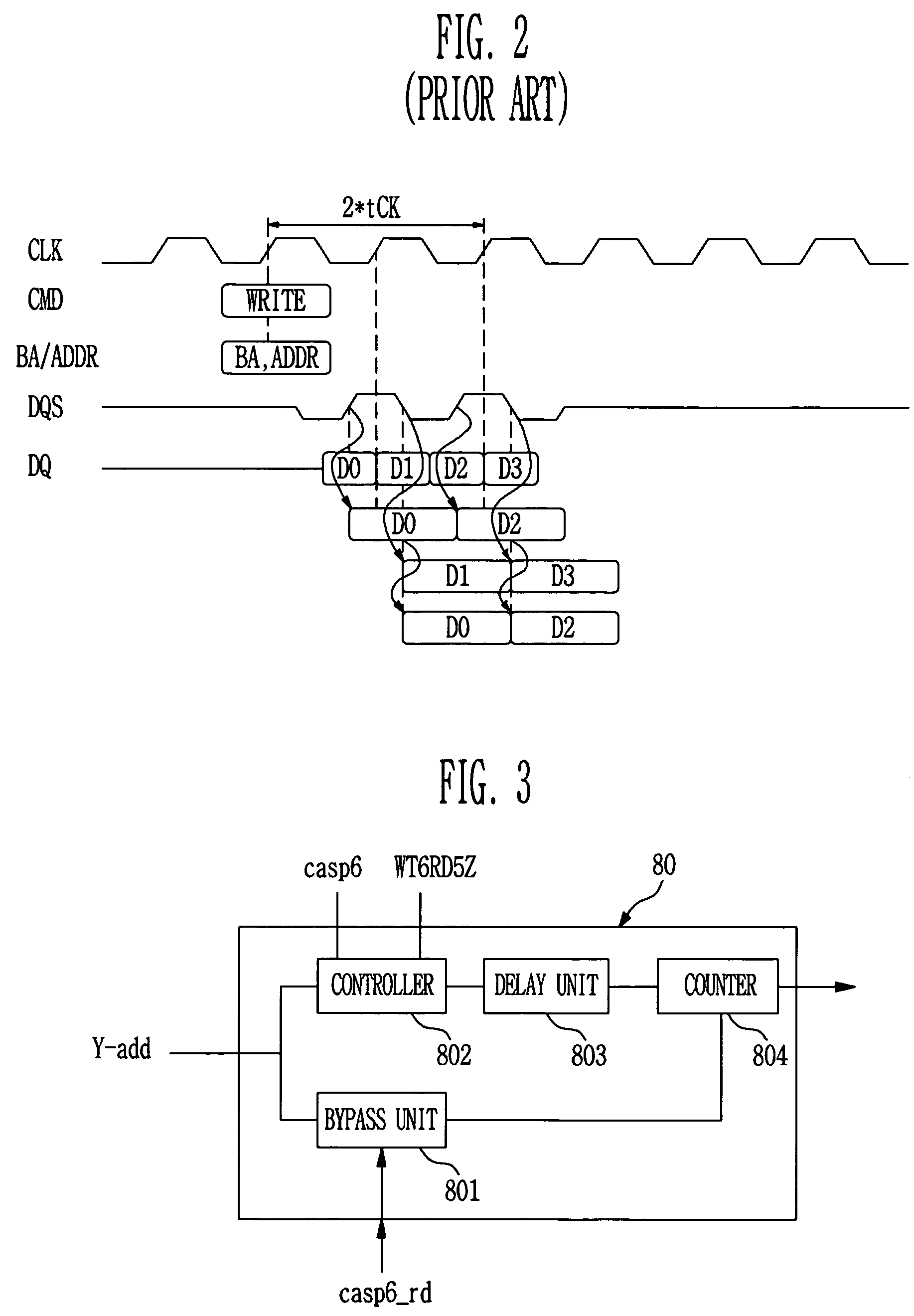
[0020]FIG. 3 is a schematic block diagram of a column address counter and a latch according to an embodiment of the present invention.

[0021]In the read operation, a control signal casp6_rd is enabled, and a column address Y-add is thus provided to a counter 804 through a bypass unit 801. A controller 802 generates a control signal according to a signal casp6, which is enabled in the write and read operations, and a signal WT6RD5Z, which is enabled in the write operation and disabled in the read operation. The column address Y-add can be provided to a delay unit 803 or block according to an output signal of the controller 802. The delay unit 803 delays the received column address Y-add by 2*tCK and provides the delayed column address to the counter 804.

[0022]That is, in the present embodiment, the delay unit 803 is not driven in the read operation but ...


PUM


Abstract

A semiconductor memory device wherein, in order to control the current consumed in a column address counter and latch block in a read operation, delay units disposed in the column address counter and latch block perform a shifting operation according to a signal CASP6, which is enabled in the write and read operations, and a signal WT6RD5Z, which is enabled in the write operation and disabled in the read operation. Accordingly, unnecessary current consumed in the read operation can be reduced.

Description

BACKGROUND[0001]1. Field of the Invention[0002]The present invention relates to a semiconductor memory device in which current consumption is reduced in a read operation, and more specifically, to a semiconductor memory device in which the current consumed in a column address counter and a latch in the read operation can be reduced.[0003]2. Discussion of Related Art[0004]FIG. 1 is a functional block diagram illustrating the configuration of a DDR SDRAM in the prior art.[0005]A control logic 10 includes a command decoder 20 and a mode register 30. A clock enable signal CKEn, a clock signal CK, a clock bar signal / CK, a chip select signal / CSn, a write enable signal / WE, a column address strobe signal / CAS and a row address strobe signal / RAS are input to the control logic 10. Further, block select addresses BA0, BA1 and addresses A0 to A13 are input to the control logic 10 through an address register 40. The command decoder 20 generates read, write and precharge commands, etc. accord...

Claims


Application Information

Patent Timeline
Patent Type & Authority Patents(United States)
IPC IPC(8): G11C7/00
CPCG11C7/1066G11C7/1072G11C7/22G11C11/4076G11C11/408G11C11/4096
Inventor SHIN, BEOM JU
Owner SK HYNIX INC
Why Eureka
Try Eureka