

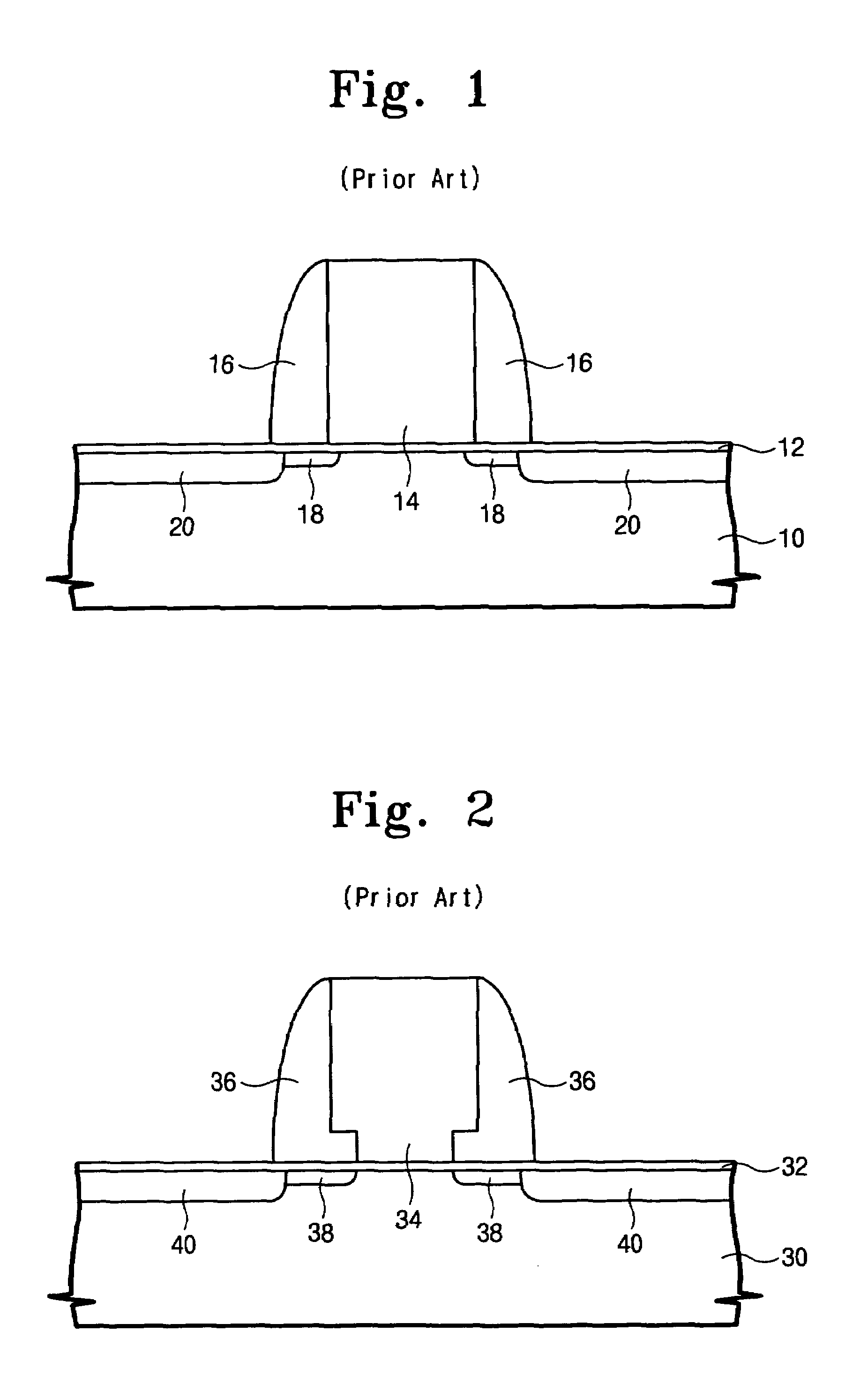
MOS transistor having a T-shaped gate electrode
a technology of metal oxidesemiconductor and gate electrode, which is applied in the manufacture of semiconductor/solid-state devices, semiconductor devices, and electrical apparatus, etc., can solve the problems of severe degradation of semiconductor device characteristics, inability to completely satisfy the requirements of high integration and high-speed characteristics, and still difficult to shrink the width of the gate pattern. , to achieve the effect of reducing the source/drain resistan
- Summary
- Abstract
- Description
- Claims
- Application Information
AI Technical Summary
Benefits of technology
Problems solved by technology
Method used
Image

Examples
Embodiment Construction
[0028]Korean Patent Application No. 2001-72687, filed on Nov. 21, 2001, and entitled: “MOS Transistor Having T-Shaped Gate Electrode and Method for Fabricating the Same,” is incorporated by reference herein in its entirety.
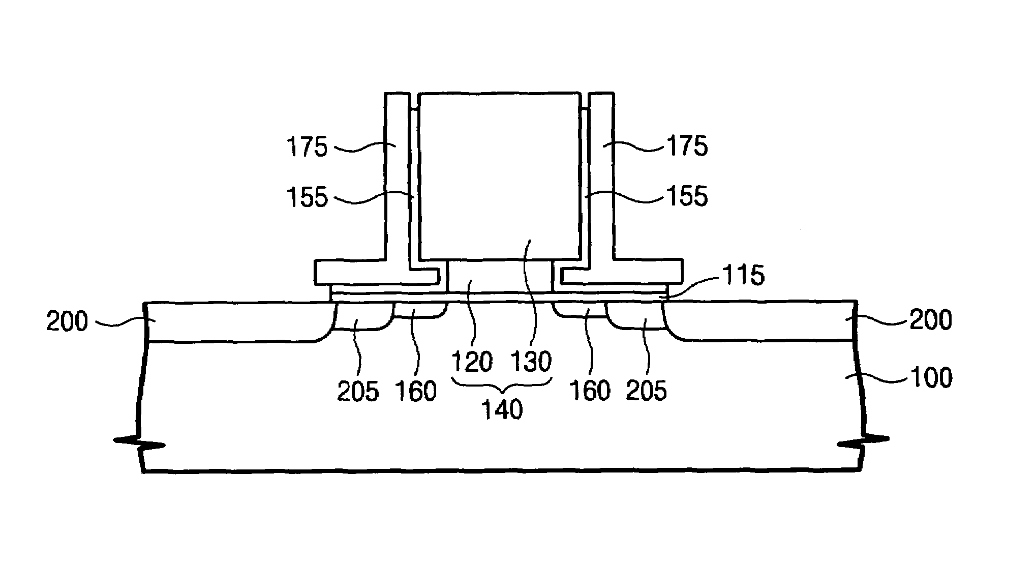
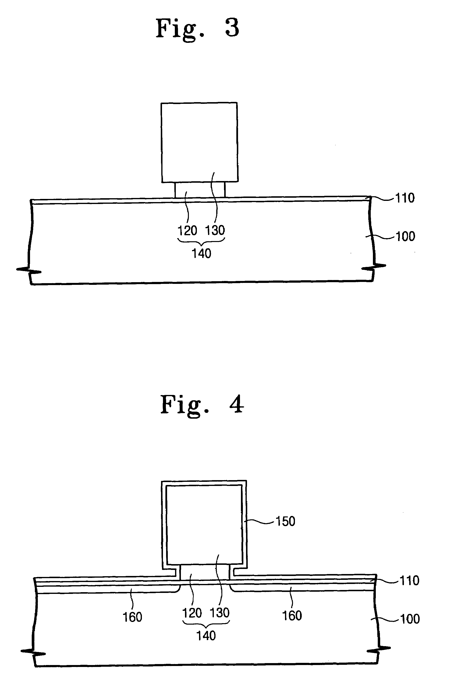
[0029]The present invention will now be described more fully hereinafter with reference to the accompanying drawings, in which preferred embodiments of the present invention are shown. The invention may, however, be embodied in different forms and should not be construed as limited to the embodiments set forth herein. Rather, these embodiments are provided so that this disclosure will be thorough and complete, and will fully convey the scope of the invention to those of ordinary skill in the art. In the attached figures, the thickness of layers and regions are exaggerated for clarity. It will also be understood that when a layer is referred to as being “on” another layer or substrate, it may be directly on the other layer or substrate, or intervening layers may al...
PUM
 Abstract
Description
Claims
Application Information