Method and system for measuring thin films

a thin film and measurement method technology, applied in the field of semiconductor manufacturing, can solve the problems of limited low spatial resolution of techniques, and significant amount of time, and achieve the effect of reducing measurement accuracy and repeatability, and facilitating optical measurements of thin film parameters

Inactive Publication Date: 2007-07-31
NOVA MEASURING INSTR LTD
View PDF1 Cites 0 Cited by
  • Summary
  • Abstract
  • Description
  • Claims
  • Application Information

AI Technical Summary

Benefits of technology

[0012]There is accordingly a need in the art to facilitates an optical measurements of thin films parameters of semiconductor workpiece, such as a semiconductor wafer, by providing a novel optical system and method for implementation a “large spot” technique in such manner that provides desired spatial resolution, especially in the edge area of the wafer, without sufficiently reducing the measurement's accuracy and repeatability.

Problems solved by technology

Performance of entire measurement cycle, i.e. including pre-measurement cycle require significant amount of time and in some cases are the bottle-neck of the equipment run rate.
Being limited in measurement accuracy and repeatability, such technique still is useful for some applications.
The main limitation of the “large spot” technique is its low spatial resolution.
For example, after CMP processing of silicon oxide layer, a high non-uniformity of the film thickness, especially in the wafer edge areas is observed.
Thus, large spot of about 20 mm and larger can not provide needed information, when resolution of about 1 mm is needed.
Reducing the spot size to the level of 1 mm will deteriorate drastically the measurement accuracy and in many cases makes this measurement impossible because of too strong dependence of received spectrum on the pattern structure.

Method used


Image

  • Method and system for measuring thin films
  • Method and system for measuring thin films
  • Method and system for measuring thin films

Examples


Embodiment Construction

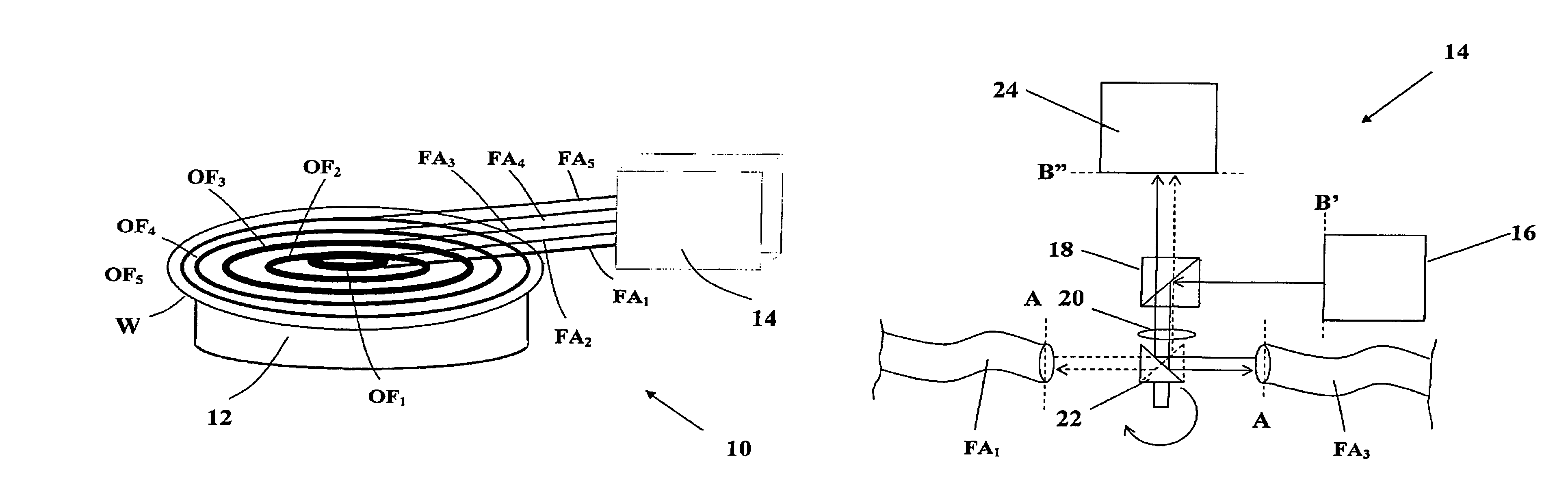
[0032]The main idea of the invention is that the light spot is configured in a form of annular ring, preferably having the same center (coincide) with the measured wafer.

[0033]The entire area of such ring-like spot is large enough, about the same as the regular circular spot of a diameter=20 mm or even greater. Since in the wafer edge vicinity the diameter of such annular ring is very large, it allows very small width of the ring and thus the high spatial resolution of the measurements near the wafer edge.

[0034]Such ring-like shape of the light spot allows measuring very accurately the thickness of radial non-uniformity that is typical for the most existing deposition and removal processes. The area Sr of ring may be calculated as Sr≈2πrΔr, wherein r is an average ring's radius and Δr—is a ring width. Lets consider Smin is the minimal area of signal collection / illumination needed for “large spot” spectral measurements. The relationship between the ring's radius r and a ring width Δr...


PUM


Abstract

An optical system is presented for use in a measurement system (100) for use in measurements of thin films of a workpiece (W), the system comprising an optical assembly (14), comprising illuminator assembly, a detector assembly, and a light directing assembly (FA-OF) for directing illuminating light to a plurality of measurement sites in the workpiece (W) arranged in an array of substantially concentric ring-like regions, such that an area defined by the measurement sites within one of the substantially concentric ring-like regions is substantially equal to that of the other substantially concentric ring-like region.

Description

FIELD OF THE INVENTION[0001]Present invention relates to the field of semiconductor manufacturing, and more specifically to the optical methods and tools for measuring thickness and optical parameters of thin films.BACKGROUND OF THE INVENTION[0002]Several optical methods are currently used for measuring thickness of thin films in semiconductor workpiece (e.g. wafer) manufacturing, mainly based on spectrophotometry and ellipsometry. There are different configurations of optical measuring tools: in-situ, performing measurements during the processing; stand-alone (SA) tools having individual cassette-to-cassette load / unload means and integrated tools, installed within or adjacent to processing equipment for layer deposition (like CVD cluster tools of Applied Materials. USA) or for layer removal (like CMP polishers of Applied Materials, EBARA, SFI, etc.) Such integrated metrology tools provide accurate measurements of each wafer immediately after the processing, e.g. layer deposition / re...

Claims


Application Information

Patent Timeline
Patent Type & Authority Patents(United States)
IPC IPC(8): G01B11/02G01B11/06
CPCG01B11/0616
Inventor FINAROV, MOSHE
Owner NOVA MEASURING INSTR LTD
Why Eureka
Try Eureka