Flash memory device including bit line voltage clamp circuit for controlling bit line voltage during programming, and bit line voltage control method thereof

programming technology, applied in static storage, digital storage, instruments, etc., can solve the problems of increasing programming disturbance, reducing programming efficiency, and reducing the voltage difference between the source and drain of the memory cell mcell, so as to reduce the change in a bit line voltage

Active Publication Date: 2007-07-31
SAMSUNG ELECTRONICS CO LTD
View PDF6 Cites 25 Cited by
  • Summary
  • Abstract
  • Description
  • Claims
  • Application Information

AI Technical Summary

Benefits of technology

[0015]The present invention also provides a bit line voltage control method capable of reducing the change in a bit line voltage during a programming operation in a flash memory device.

Problems solved by technology

However, in the flash memory device described above, if the bit line voltage VBL becomes higher than a desired voltage, the voltage difference between the source and drain of the memory cell MCELL becomes smaller, which reduces programming efficiency.
On the contrary, if the bit line voltage VBL becomes lower than the desired voltage, a voltage difference between the source and drain of a memory cell that is adjacent to the memory cell MCELL and shares the bit line and source line increases, which increases programming disturbance.

Method used


Image

  • Flash memory device including bit line voltage clamp circuit for controlling bit line voltage during programming, and bit line voltage control method thereof
  • Flash memory device including bit line voltage clamp circuit for controlling bit line voltage during programming, and bit line voltage control method thereof
  • Flash memory device including bit line voltage clamp circuit for controlling bit line voltage during programming, and bit line voltage control method thereof

Examples


Embodiment Construction

[0030]Hereinafter, embodiments of the present invention will be described in detail with reference to the appended drawings. The same reference numbers refer to the same components throughout the drawings.

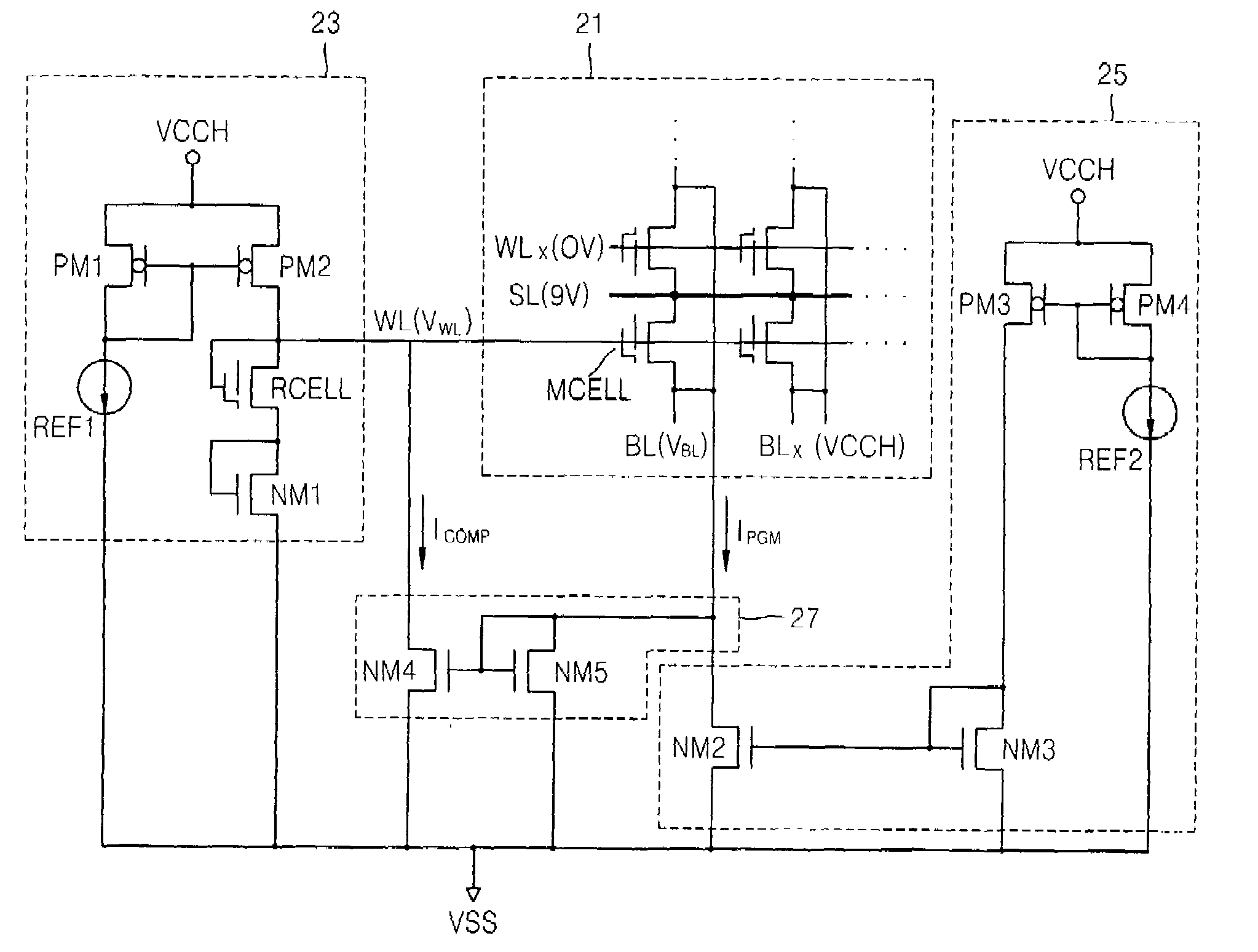
[0031]FIG. 2 is a circuit diagram of a flash memory device according to an embodiment of the present invention.

[0032]Referring to FIG. 2, the flash memory device comprises a flash memory cell array 21, a word line voltage generation circuit 23, a program current generation circuit 25, and a bit line voltage clamp circuit 27.

[0033]The flash memory cell array 21 includes a plurality of flash memory cells MCELLs. The source of each flash memory cell MCELL is connected to a source line SL, the bit line thereof is connected to a bit line BL, and the gate thereof is connected to a word line WL.

[0034]The word line voltage generation circuit 23 is connected to the word line WL to generate and provide a word line voltage VWL to the word line WL. The word line voltage generation circuit 23, ...


PUM


Abstract

In a flash memory device and a bit line voltage control method thereof a circuit capable of reducing the change in a voltage of a bit line during programming. The flash memory device includes: a flash memory cell, a source of which is connected to a source line, a drain of which is connected to a bit line and a gate of which is connected to a word line; a word line voltage generation circuit connected to the word line, for generating and providing a word line voltage to the word line; a program current generation circuit connected to the bit line, for generating and providing a program current to the bit line; and a bit line voltage clamp circuit connected to the bit line and the word line, for sensing a voltage of the bit line and controlling a bias current of the word line voltage generation circuit to thereby control a voltage of the bit line, during a programming operation of the flash memory device. Therefore, it is possible to enhance program efficiency and reduce program disturbance by constantly maintaining the voltage of the bit line to a desired voltage using a bit line voltage clamp circuit during programming.

Description

BACKGROUND OF THE INVENTION[0001]This application claims the priority of Korean Patent Application No. 2004-46952, filed on Jun. 23, 2004, in the Korean Intellectual Property Office, the disclosure of which is incorporated herein in its entirety by reference.FIELD OF THE INVENTION [0002]The present invention relates to a flash memory device, and more particularly, to a bit line voltage clamp circuit for controlling a bit line voltage during programming in a flash memory device, and a bit line voltage control method thereof.DESCRIPTION OF THE RELATED ART[0003]Flash memory devices have enjoyed widespread use in various electronic systems, such as mobile systems. FIG. 1 is illustrates circuitry related to program operations in a conventional flash memory device. Referring to FIG. 1, a flash memory cell array 11 includes a plurality of flash memory cells MCELLs. The source of each flash memory cell MCELL is connected to a source line SL, the drain thereof is connected to a bit line BL, ...

Claims


Application Information

Patent Timeline
Patent Type & Authority Patents(United States)
IPC IPC(8): G11C11/34G11C5/14G11C16/04G11C16/24
CPCG11C5/145G11C16/0425G11C16/24G11C16/3427G11C16/08G11C16/12
Inventor O, SE-EUN
Owner SAMSUNG ELECTRONICS CO LTD
Why Eureka
Try Eureka