Semiconductor device and manufacturing method thereof

a semiconductor and manufacturing method technology, applied in the direction of semiconductor devices, electrical devices, transistors, etc., can solve the problems of inconvenient mass production, affecting the enhancement of performance by reducing the thickness affecting the performance of the gate insulator,

Inactive Publication Date: 2007-08-07
SEMICON TECH ACADEMIC RES CENT
View PDF8 Cites 22 Cited by
  • Summary
  • Abstract
  • Description
  • Claims
  • Application Information

AI Technical Summary

Benefits of technology

[0012]According to an aspect of the invention, a MOS semiconductor device manufacturing method comprises forming an device region of a first conductivity type for forming first MOS semiconductor element devices and a device region of a second conductivity type for forming second MOS semiconductor element devices in a semiconductor substrate, forming a gate insulator, forming a laminated film comprising a molybdenum film and a nitrogen containing film which is to be used to dope nitrogen into the molybdenum film, doping nitrogen from the nitrogen containing film into the molybdenum film, processing the laminated film into gate electrodes of the first and second MOS semiconductor element devices, removing the nitrogen containing film from the gate electrodes of the second MOS semiconductor element device and covering the gate electrode of the first MOS semiconductor element devices with a nitrogen diffusion preventing film, and reducing the nitrogen concentration in the molybdenum film of the gate electrodes of the second MOS semiconductor element device.
[0013]In another aspect of the invention, a MOS semiconductor device manufacturing method comprises forming an device region of a first conductivity type for forming first MOS semiconductor element devices and an device region of a second conductivity type for forming second MOS semiconductor element devices in a semiconductor substrate, sequentially forming a gate insulator and a molybdenum film, processing the molybdenum film into gate electrodes of the first and second MOS semiconductor element devices, forming a nitrogen containing film which is to be used to dope nitrogen into the molybdenum film of the gate electrodes, doping nitrogen into the molybdenum film from the nitrogen containing film, removing the nitrogen containing film from the gate electrodes of the second MOS semiconductor element devices and covering the gate electrodes of the first MOS semiconductor element devices with a nitrogen diffusion preventing film, and reducing the nitrogen concentration in the molybdenum film of the gate electrodes of the second MOS semiconductor element devices.

Problems solved by technology

However, the influence of the depletion layer formed in the polysilicon gate electrode has caused a more serious problem as devices have become further miniaturized in recent years.
Further, enhancement of the performance by a reduction in the gate insulator thickness may be hindered.
However, when this technique is applied to a CMOS semiconductor device production in practice, the manufacturing process becomes too complicated and is not suitable for mass production.
However, it has been pointed out problems by the inventors and others based on their studies.
That is, this method is not practical because of problems that the gate insulator and an interface between the gate electrode and the gate insulator are damaged in the implantation.
However, no study of a method for applying the technique to a CMOS semiconductor device with gate electrodes adjusting to have different work function values on the same semiconductor substrate has been reported.

Method used


Image

  • Semiconductor device and manufacturing method thereof
  • Semiconductor device and manufacturing method thereof
  • Semiconductor device and manufacturing method thereof

Examples


first embodiment

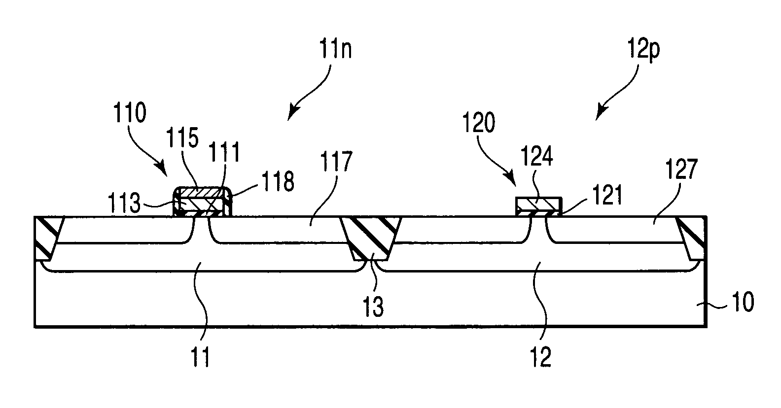
[0042]A first embodiment relates to a manufacturing method for a CMOS semiconductor device with a basic structure, that is a method for doping nitrogen into an entire Mo film used to gate electrodes before patterning the gate electrodes and then out-diffusing nitrogen from the gate electrodes of only one type to reduce the nitrogen concentration.

[0043]FIGS. 1 to 5 are cross sectional views showing a manufacturing method for a MOS semiconductor device according to the first embodiment of the invention.

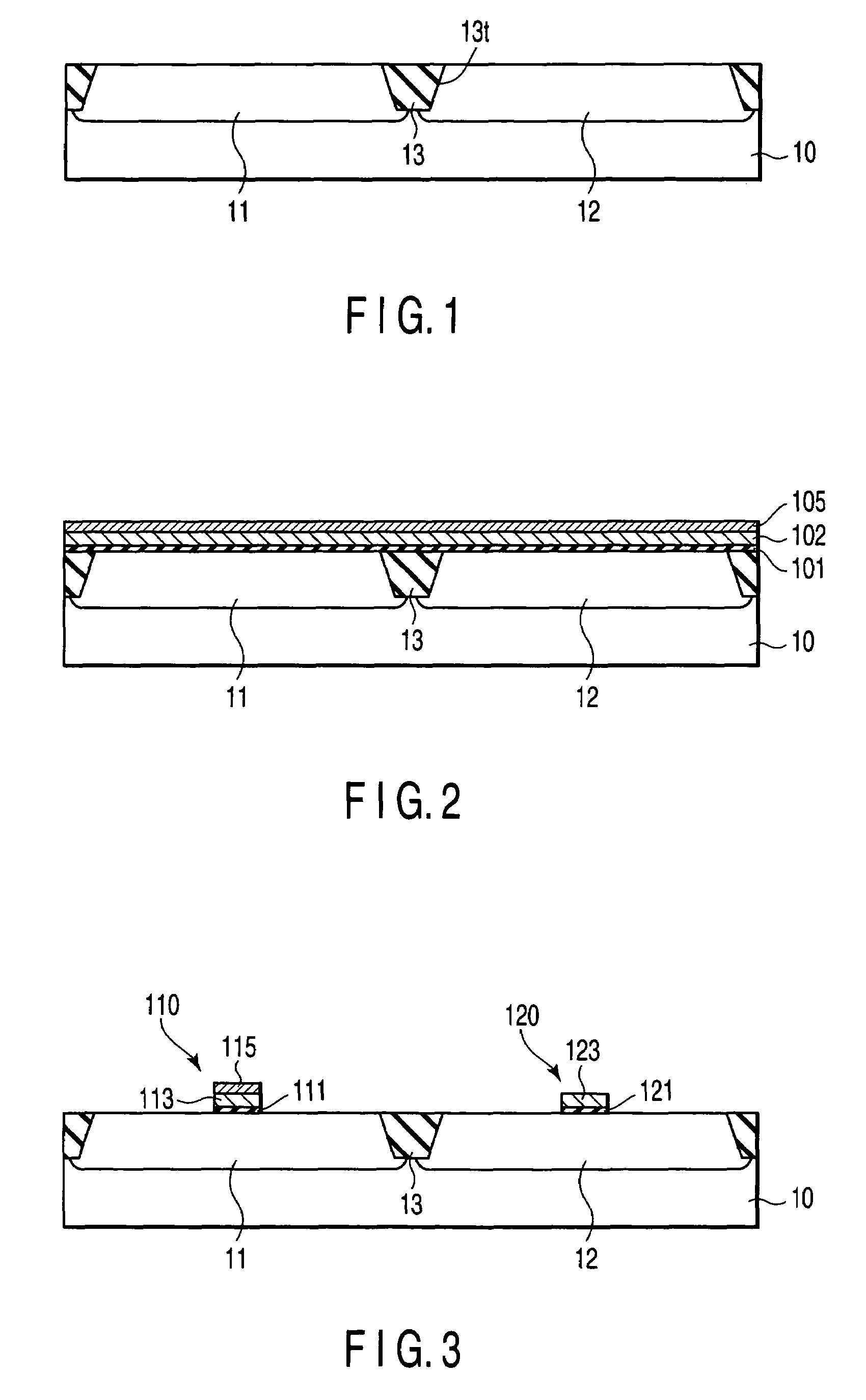
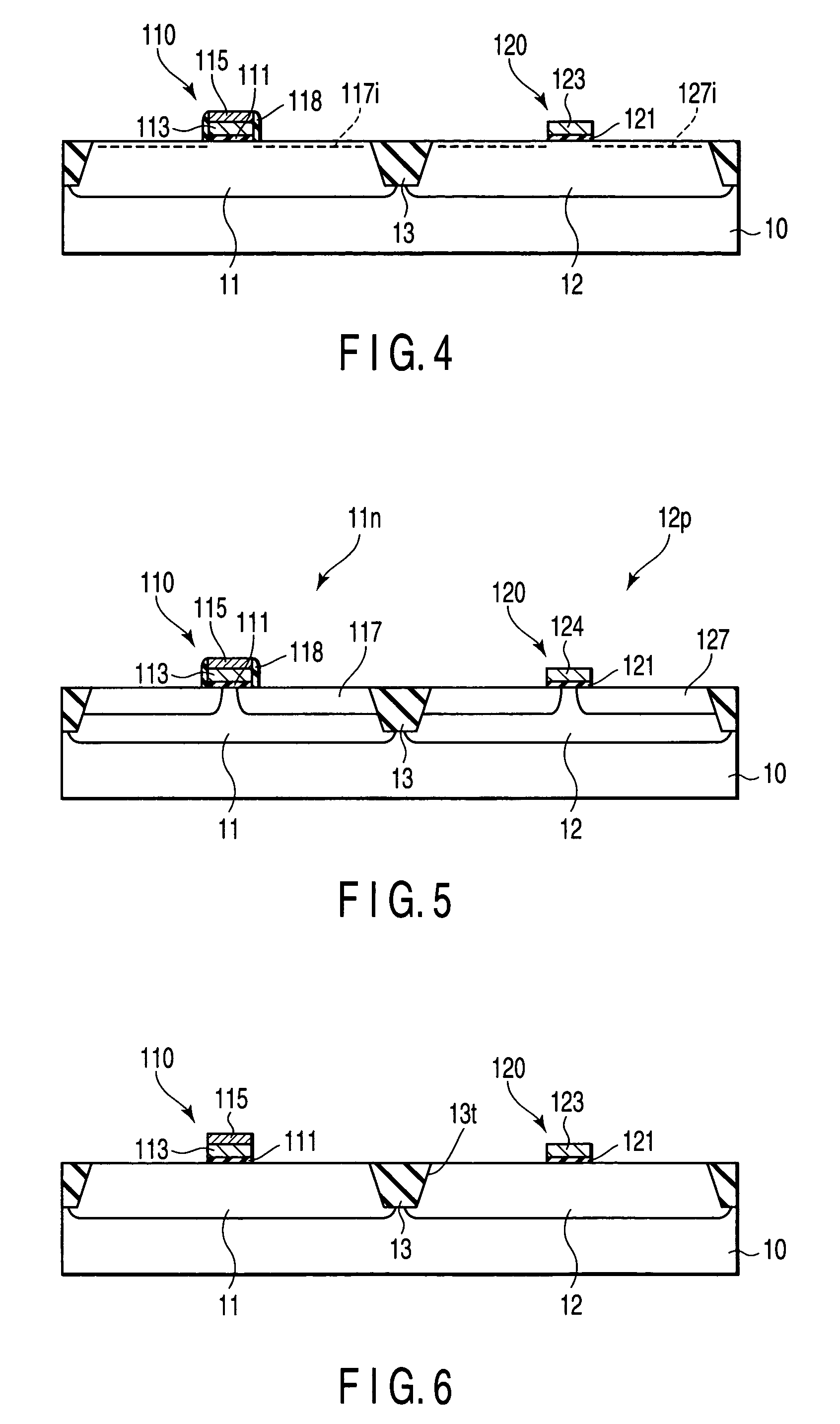
[0044]First, as shown in FIG. 1, a first conductivity type, for example, p-type, semiconductor device region 11 and a second conductivity type, for example, n-type, semiconductor device region 12, and an isolation 13 for isolating adjacent semiconductor devices from each other are formed in a silicon substrate 10. As the silicon substrate 10, a p-type substrate is used in many cases, but an n-type substrate can also be used. In this case, the manufacturing process is basically the same ...

second embodiment

[0061]A second embodiment relates to a manufacturing method for a CMOS semiconductor device having regions with shallower junction depth formed near gate edges (hereinafter referred to as extensions) to relax the short channel effect of a MOS semiconductor device. Similar to the first embodiment, nitrogen is doped into an entire Mo film before gate electrode patterning and then nitrogen is out-diffused from the gate electrodes of only one of the MOS devices.

[0062]FIGS. 6 to 8 are cross sectional views showing the steps of a manufacturing method for a MOS semiconductor device according to the second embodiment of the invention. In this embodiment, the process up to the step of forming the gate electrode structures 110, 120 is the same as that of the first embodiment. Therefore, the process up to the gate electrode formation is briefly explained below, but the detail explanation is omitted.

[0063]FIG. 6 is the same as FIG. 3. First and second semiconductor device regions 11, 12 and an ...

third embodiment

[0073]Like the first embodiment, a third embodiment relates to a manufacturing method for a CMOS semiconductor device in which no extensions are formed. However, in the third embodiment, nitrogen is doped into both gate electrodes after gate electrode structures are formed and then nitrogen is out-diffused from the gate electrodes of only one of the CMOS devices.

[0074]FIGS. 9 to 12 are cross sectional views showing the steps of a manufacturing method for a MOS semiconductor device according to the third embodiment of the invention. As shown in FIG. 9, first and second semiconductor device regions 11, 12 and an isolation 13 to isolate the adjacent semiconductor devices from each other are formed on a silicon substrate 10. Further, a gate insulator 101 and a Mo film 102 for forming gate electrodes are formed on an entire surface of the resultant structure. In this embodiment, the process up to the step of forming the Mo film 102 is the same as that of the first embodiment, and therefo...


PUM

PropertyMeasurementUnit
thicknessaaaaaaaaaa
feature sizeaaaaaaaaaa
thicknessaaaaaaaaaa

Abstract

A manufacturing method for a CMOS semiconductor device in which gate electrodes are adjusted to have different work function values comprises forming an device region of a first and second conductivity type for forming first and second MOS semiconductor element devices, respectively, in a semiconductor substrate, forming a gate insulator, forming a laminated film comprising a molybdenum film and nitrogen containing film for doping nitrogen into molybdenum, doping nitrogen from the nitrogen containing film into molybdenum, processing the laminated film into gate electrodes of the first and second MOS semiconductor element devices, removing the nitrogen containing film from the gate electrodes of the second MOS semiconductor element device and covering the gate electrode of the first MOS semiconductor element devices with a nitrogen diffusion preventing film, and reducing the nitrogen concentration in molybdenum of the gate electrodes of the second MOS semiconductor element device.

Description

CROSS-REFERENCE TO RELATED APPLICATIONS[0001]This application is based upon and claims the benefit of priority from prior Japanese Patent Application No. 2003-311387, filed Sep. 3, 2003, the entire contents of which are incorporated herein by reference.BACKGROUND OF THE INVENTION[0002]1. Field of the Invention[0003]The invention relates to a MOS semiconductor device and a manufacturing method thereof, more particularly, to a MOS semiconductor device in which work functions of gate electrodes are adjusted to different values for MOS transistors having different conductivity types in a dual-gate structure using a metal as a gate electrode and a manufacturing method thereof.[0004]2. Description of the Related Art[0005]In a miniaturized CMOS semiconductor device, it is general to use a so-called dual-gate structure. In the dual-gate structure, a polysilicon highly doped with an n-type impurity (dopant) (hereinafter referred to as n+ polysilicon), for example, phosphorus, is used to a ga...

Claims


Application Information

Patent Timeline
Patent Type & Authority Patents(United States)
IPC IPC(8): H01L29/78H01L29/43H01L21/8238H01L21/28H01L27/092H01L29/423H01L29/49
CPCH01L21/823842
Inventor SHIBAHARA, KENTARO
Owner SEMICON TECH ACADEMIC RES CENT
Why Eureka
Try Eureka