Joined body of piezoelectric material substrate and support substrate, and acoustic wave element

a piezoelectric material and acoustic wave technology, applied in the direction of impedence networks, electrical apparatus, piezoelectric/electrostrictive/magnetostrictive devices, etc., can solve the problems of deterioration of the characteristics of the thus obtained bonded body, low characteristic, and low crystallinity, etc., to achieve deterioration of the bonded body, high sound speed, and high nitrogen concentration

Active Publication Date: 2020-10-01
NGK INSULATORS LTD
View PDF3 Cites 2 Cited by
  • Summary
  • Abstract
  • Description
  • Claims
  • Application Information

AI Technical Summary

Benefits of technology

[0035]The inventors have researched the reason that the characteristic of the bonded body is deteriorated when the piezoelectric material substrate composed of lithium niobate or the like and the supporting substrate with the silicon oxide layer are directly bonded with each other. Particularly, it is studied in detail the reason that a ratio (admittance ratio) of an admittance at a resonance frequency fs with respect to an admittance at an anti-resonance frequency fr is reduced.
[0036]In the case that the bonding layer between the piezoelectric material substrate and supporting substrate is made of silicon oxide, a sound speed of bulk wave propagating in the silicon oxide (bonding layer) is lower than a sound speed of bulk wave propagating in the piezoelectric material substrate (for example lithium niobate or lithium tantalate). It is thus considered that propagating energy is leaked from the piezoelectric material substrate into the supporting substrate through the bonding layer to deteriorate the propagation characteristics.
[0037]Here, the inventors reached the idea of providing a part having a relatively high nitrogen concentration and having a relatively high sound speed on the side of the piezoelectric material substrate of the bonding layer and of providing a part having a relatively low nitrogen concentration and low sound speed on the side of the supporting substrate. As a result, it is found that the leakage of an acoustic wave propagating in the piezoelectric material substrate into the supporting substrate can be suppressed.
[0038]Further, the inventors reached the idea of providing a part having a relatively high nitrogen concentration and a relatively high sound speed in the intermediate part of the bonding layer...

Problems solved by technology

As described in the prior documents, in the case that as piezoelectric device is produced by thinning a lithium niobate or lithium tantalate substrate by ion injection, the characteristics is low which is problematic.
It is considered that ...

Method used


Image

  • Joined body of piezoelectric material substrate and support substrate, and acoustic wave element
  • Joined body of piezoelectric material substrate and support substrate, and acoustic wave element
  • Joined body of piezoelectric material substrate and support substrate, and acoustic wave element

Examples


example a1

Inventive Example A1

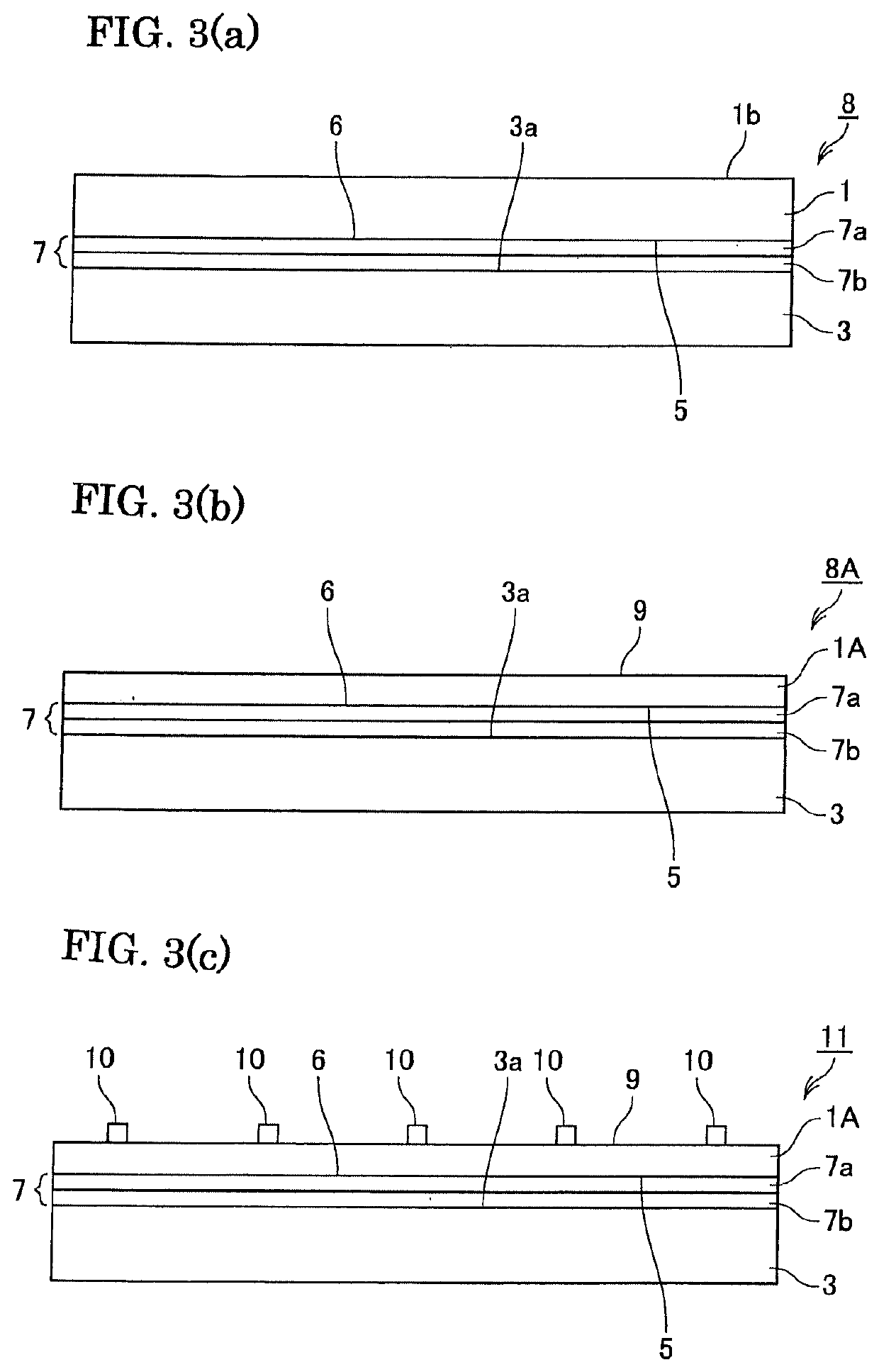
[0090]It was produced an acoustic wave device 11 shown in FIG. 3(c), according to the method described referring to FIGS. 1 to 3.

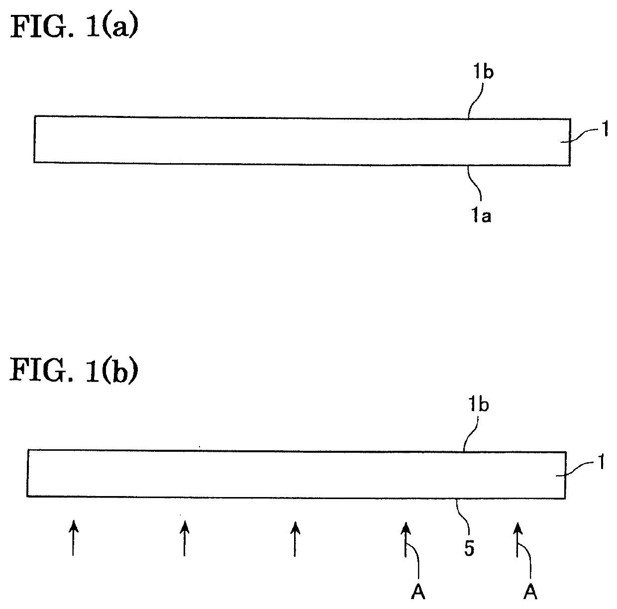
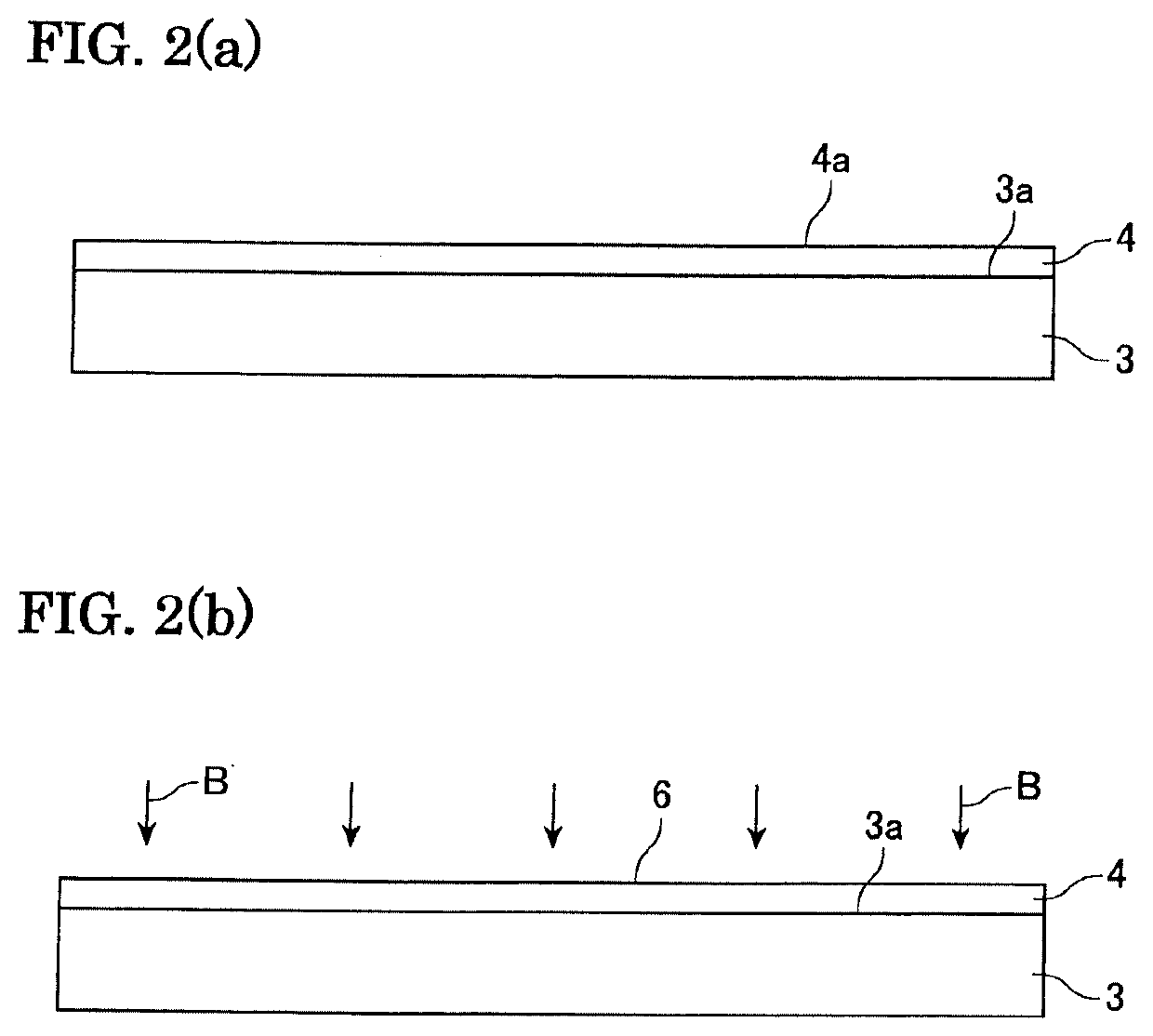
[0091]Specifically, it was prepared a 42Y-cut X-propagation LiTaO3 substrate (piezoelectric material substrate) 1 having a thickness of 200 μm and both main faces polished into mirror surfaces and a high-resistance (>2 kΩ·cm) Si (100) substrate (supporting substrate) 3 having a thickness of 675 μm. Both substrates have sizes of 150 mm, respectively. A silicon oxide layer 4 was film-formed by sputtering in a thickness of 500 nm on the supporting substrate 4. As the silicon oxide layer 4 after the film-formation had a surface roughness Ra of 0.6 nm, the surface was slightly polished by CMP (Chemical mechanical polishing) so that Ra was improved to 0.3 nm.

[0092]The bonding face 1a of the piezoelectric material substrate 1 and the bonding face 4a of the silicon oxide layer on the supporting substrate 3 were subjected to cleaning and surface...

example a2

Inventive Example A2

[0096]In the inventive example A1, plasma of mixed gases of 80 percent of nitrogen gas and 20 percent of oxygen gas was used instead of nitrogen plasma. When the gas composition was changed, the matching was appropriately changed so that the reflection electric power took the minimum value. The other conditions were the same as those in the inventive example A1.

[0097]According to same procedure as the inventive example A1, nitrogen concentrations, carbon concentrations and fluorine concentrations at the respective parts in the thus obtained bonded body 8 were measured and the measurement results were shown in table 1. Further, as the inventive example A1, the piezoelectric material substrate was processed so that the thickness of the piezoelectric material substrate 1A was made 16, 8, 4, 2 or 1 μm. The ratio of the admittance value at the resonance frequency fs with respect to the admittance value at the anti-resonance frequency fr was measured. The results were ...

example b

Inventive Example B

[0101]In the inventive example A1, the material of the piezoelectric material substrate was changed to a 128Y-cut X-propagation lithium niobate. As a result, it was obtained the same results as those of the inventive example A1.

Inventive Example C1

[0102]It was produced an acoustic wave device 21 shown in FIG. 5(c), according to the method illustrated referring to FIGS. 2, 4 and 5.

[0103]Specifically, it was prepared a 42Y-cut X-propagation LiTaO3 substrate (piezoelectric material substrate) 1 having a thickness of 200 μm and both main faces polished into mirror surfaces and a high-resistance (>2 kΩ·cm) Si (100) substrate (supporting substrate) 3 having a thickness of 675 μm. Both substrates have sizes of 150 mm, respectively. Silicon oxide films 12 and 4 were film-formed by sputtering in thicknesses of 250 nm on the piezoelectric material substrate 1 and supporting substrate 3, respectively. As the respective silicon oxide films 12 and 4 after the film-formation ea...


PUM


Abstract

A bonded body includes a supporting substrate, a piezoelectric material substrate of a material selected from the group consisting of lithium niobate, lithium tantalate and lithium niobate-lithium tantalate, and a bonding layer bonding the supporting substrate and piezoelectric material substrate. The material of the bonding layer is silicon oxide. Provided that the bonding layer is divided into a piezoelectric material substrate-side bonding part and supporting substrate-side bonding part, the piezoelectric material substrate-side bonding part has a nitrogen concentration higher than a nitrogen concentration of the supporting substrate-side bonding part.

Description

CROSS-REFERENCE TO RELATED APPLICATIONS[0001]This application is a continuation application of PCT / JP2018 / 042433, filed Nov. 16, 2018, which claims priority to Japanese Application No. 2017-252872, filed Dec. 28, 2017, the entire contents all of which are incorporated hereby by reference.TECHNICAL FIELD[0002]The present invention relates to a bonded body of a piezoelectric material substrate and supporting substrate, and an acoustic wave device.BACKGROUND ARTS[0003]It has been widely used an SOI substrate composed of a high resistance Si / SiO2 thin film / Si thin film, for realizing a high-performance semiconductor device. Plasma activation is used for realizing the SOI substrate. This is because the bonding can be realized at a relatively low temperature (400° C.). It is proposed a composite substrate composed of similar Si / SiO2 thin film / piezoelectric thin film for improving the characteristics of a piezoelectric device (patent document 1). According to patent document 1, the piezoel...

Claims


Application Information

Patent Timeline
IPC IPC(8): H03H9/02H01L41/312H01L41/337H03H3/08H03H9/25
CPCH03H9/02574H03H9/02559H03H9/25H01L41/312H01L41/337H03H3/08H10N30/073H10N30/88H10N30/20H10N30/853H10N30/01H10N30/072H10N30/086
Inventor HORI, YUJIYAMADERA, TAKAHIROTAKAGAKI, TATSURO
Owner NGK INSULATORS LTD
Why Eureka
Try Eureka