Multiplier and shift device using signed digit representation

a multiplication device and digit representation technology, applied in the field of multiplication devices and shifters, can solve the problems of limiting the applicability of the multiplier device to multiplication by only the fixed amount, increasing the amount of (control) hardware, and the achievable complexity reduction is still not optimal, so as to reduce the number of necessary additions, reduce the area needed, and reduce the number of necessary shifting operations

Inactive Publication Date: 2007-08-14
NOKIA SOLUTIONS & NETWORKS OY
View PDF11 Cites 27 Cited by
  • Summary
  • Abstract
  • Description
  • Claims
  • Application Information

AI Technical Summary

Benefits of technology

[0054]In view of the above, the present invention provides a multiplier device and a shifter which are free from the above mentioned drawbacks and which enable a multiplier device and a shifter to be constituted with a minimum amount of hardware, thus consuming only a minimum area of semiconductor chip area.
[0070]Thus, with the present invention being implemented, the following advantages can be obtained:
[0071]The present invention can be used in applications using digital multiplication, such as in digital signal processing DSP, digital filters and / or finite impulse response filters FIR filters as well as programmable and / or adaptive digital filters. As the multiplier is represented in CSD coding, the number of necessary shifting operations can be reduced and the number of necessary additions can be reduced, thus contributing to a reduced area needed for a hardware realization of a shifter and a multiplier device on a silicon chip.
[0072]The multiplication of different powers of two is performed serially in time (not in parallel) in order to further reduce the area needed for a hardware realization. By virtue thereof, it is enabled to use only one adder in connection with the multiplication which contributes to a reduced hardware amount and reduced required area for the hardware.
[0073]A shifter based on binary weighted shifting is used for shifting in connection with the multiplication, thereby reducing the required hardware amount (number of multiplexers and hardwired shifting elements) and thus reducing the area for hardware implementation still further.

Problems solved by technology

However, this limits the applicability of the multiplier device to multiplications by only the fixed multiplier value.
Thus, also such a multiplier device using parallel addition requires numerous adder means and numerous shifting means, that is a bulky hardware, in order to be suitable for performing the multiplication by a variable multiplier.
However, in order to accomplish this goal, functionally correct control circuits have to be generated and implemented, thereby leading to an increased amount of (control) hardware.
However, studies of the present inventors revealed that the achievable complexity reductions are still not optimum.
This, however, causes considerable delay, which is suggested to be compensated by an (additional) pipeline register.
This, however, does not support the complexity to be reduced to a minimum.
However, processing of a multiplier being represented in CSD format is not considered.
Hence, also this prior art arrangement requires quite a bulky hardware which consumes quite significant area when implemented on a silicon chip.
In consequence, such arrangements are quite bulky and consume lots of semiconductor chip area, which is undesired in view of the aim to miniaturize IC chip designs.
Also, the costs for such devices increase with an increase in the consumed chip area.

Method used


Image

  • Multiplier and shift device using signed digit representation
  • Multiplier and shift device using signed digit representation
  • Multiplier and shift device using signed digit representation

Examples


Embodiment Construction

[0081]Subsequently, embodiments of the present invention are described in detail with reference to the drawings.

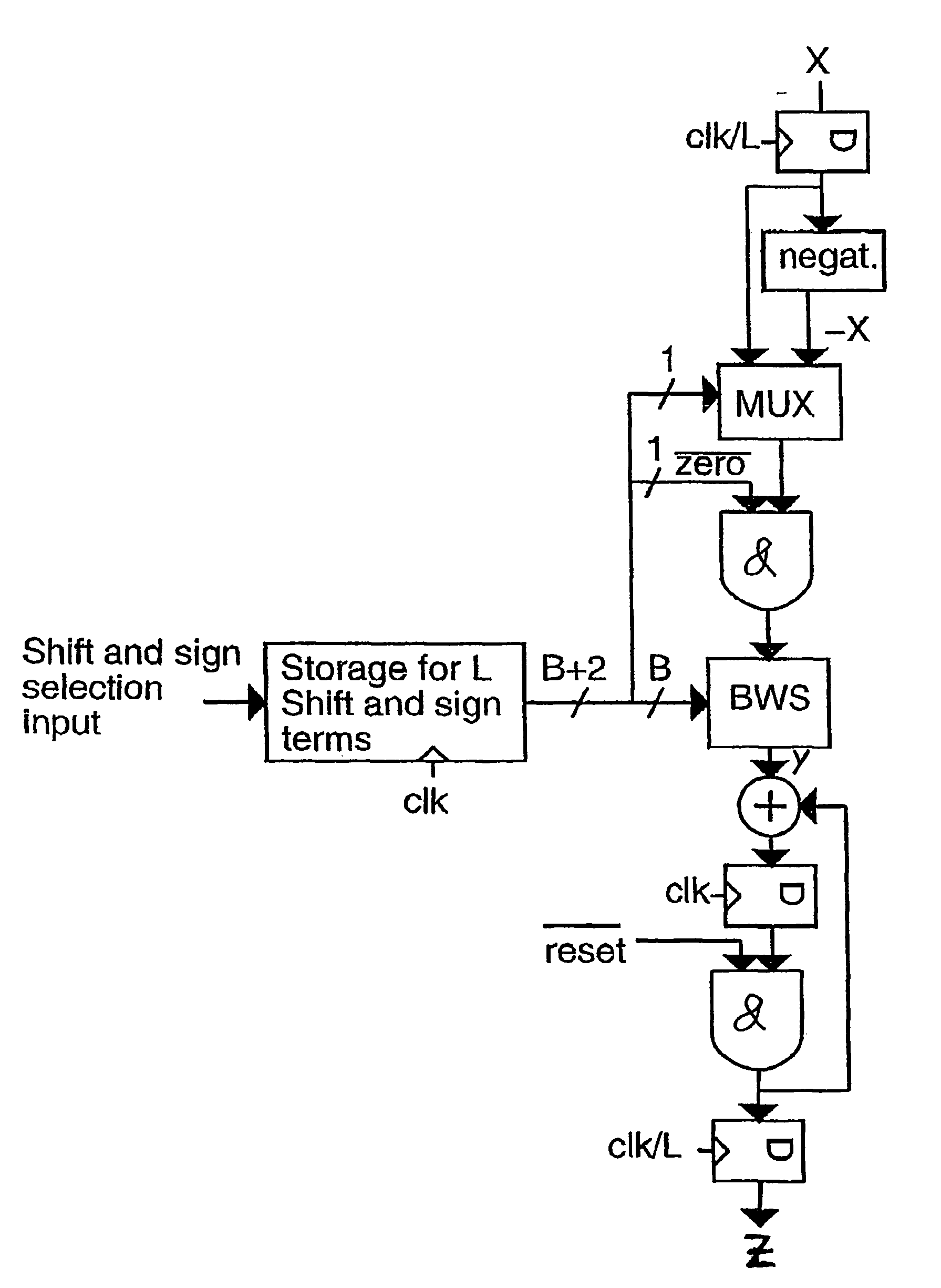
[0082]One aspect of the present invention when reducing the hardware amount and thus area needed for a multiplier device is to minimize the hardware needed for a shifter.

[0083]According to the present invention, such a minimized shifter in terms of hardware is shown in FIG. 3.

[0084]Generally, the shifts are presented serially and each stage realizes two different shift values, i.e. 0 or 2(k−1) with k being the index (number) of the stage and k reaching from 0 to B. B represents the maximum number of stages required and is linked to the bit number of the input signal (e.g. the multiplier if applied to a multiplier device) such that the input signal (multiplier) has 2B bits. The shifts of each stage are thus binary weighted in relation to each other. With such a structure, any shift amount between zero and 2B−1 can be achieved, using B multiplexers only (generally, using log...


PUM


Abstract

The present invention proposes a multiplier device performing multiplication of different powers of two serially in time (not in parallel) in order to further reduce the area needed for a hardware realization. By virtue thereof, it is enabled to use only one adder in connection with the multiplication which contributes to a reduced hardware amount and reduced required area for the hardware. A shifter means based on binary weighted shifting is used for shifting in connection with the multiplication, thereby reducing the required hardware amount (number of multiplexers and hardwired shifting elements) and thus reducing the area for hardware implementation still further. The present invention can be used in applications using digital multiplication, such as in digital signal processing DSP, digital filters and / or finite impulse response filters FIR filters as well as programmable and / or adaptive digital filters. As the multiplier is represented in CSD coding, the number of necessary shifting operations can be reduced and the number of necessary additions can be reduced, thus contributing to a reduced area needed for a hardware realization of a shifting means and a multiplier device on a silicon chip.

Description

BACKGROUND OF THE INVENTION[0001]1. Field of the Invention[0002]The present invention relates to a multiplier device and to a shifter.[0003]2. Description of the Prior Art[0004]With the spreading of digital signal processing, a need for multiplier devices which multiply digital signals has arisen.[0005]Conventionally, when multiplying two digital signals each of which representing a number value, the multiplication is performed as follows. Assume A to represent the multiplicand and B to represent the multiplier, and assume further, for example only, that A and B, respectively, are in a 4 bit representation (generally, a n-bit representation) (a bit being also referred to as digit).[0006]For multiplying (in decimal system) A=11 by B=7 (which yields 77 in decimal notation), the following has to be effected if A, B are binary signals.[0007]For each bit of the multiplier, the value of the multiplicand is to be shifted by a number of bits, which number of bits corresponds to the signific...

Claims


Application Information

Patent Timeline
Patent Type & Authority Patents(United States)
IPC IPC(8): G06F15/00G06F7/52G06F5/01
CPCG06F5/015G06F7/5272G06F7/533G06F9/3001G06F9/30025
Inventor KOSUNEN, MARKOHALONEN, KARI
Owner NOKIA SOLUTIONS & NETWORKS OY
Why Eureka
Try Eureka