Method for manufacturing an organic electroluminescence display

a manufacturing method and electroluminescence technology, applied in the direction of tube/lamp factory adjustment, identification means, instruments, etc., can solve the problems of lowering the display performance, affecting the display performance, and affecting the appearance of the organic light emission layer, so as to achieve the effect of efficient manufacturing of excellent display performan

Active Publication Date: 2007-08-21
SAMSUNG DISPLAY CO LTD +1
View PDF8 Cites 17 Cited by
  • Summary
  • Abstract
  • Description
  • Claims
  • Application Information

AI Technical Summary

Benefits of technology

[0009]In view of the above, an object of the present invention is to provide a method for manufacturing a video display, which can efficiently manufacture an organic EL display excellent in display performance.
[0011]According to the invention, an organic EL display excellent in display performance can be manufactured efficiently.

Problems solved by technology

Since this requires an additional step, the steps for manufacturing an organic EL display device are complicated.
On the other hand, according to the technique described in Patent Document 1, since foreign matter is directly irradiated with laser, it causes abrasion to possibly contaminate the organic light emission layer.
Such contamination possibly causes lowering of the display performance (for example, optical characteristics such as luminance and device life) of the organic display device.

Method used


Image

  • Method for manufacturing an organic electroluminescence display
  • Method for manufacturing an organic electroluminescence display
  • Method for manufacturing an organic electroluminescence display

Examples


Embodiment Construction

[0026]A preferred embodiment according to the present invention will below be described with reference to the accompanying drawings.

[0027]At first, a description is to be made of manufacturing steps for an organic EL display according to the embodiment with reference to an example of a bottom emission type organic EL display as an object of manufacture.

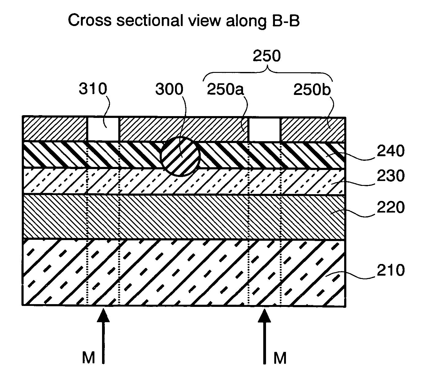
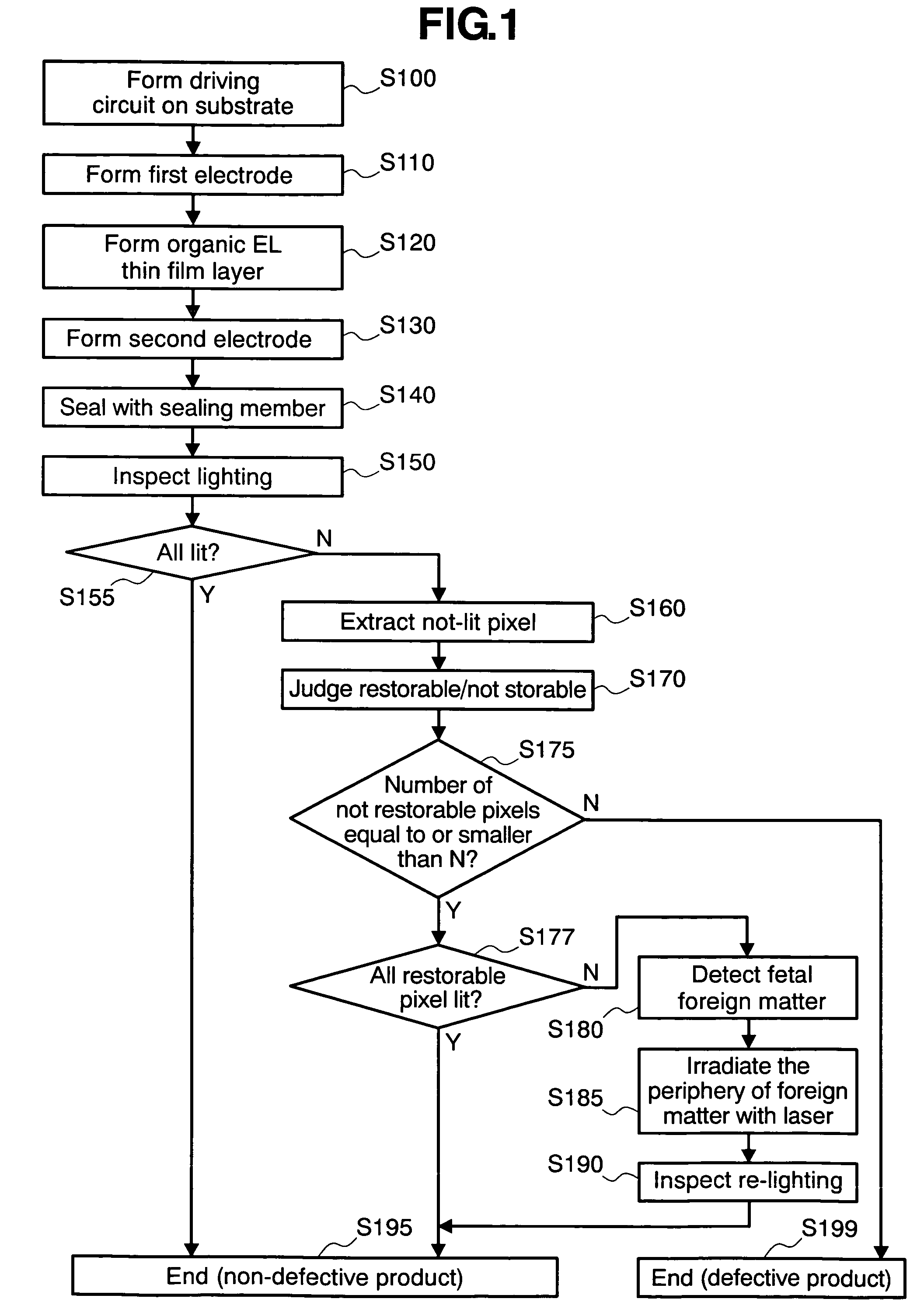
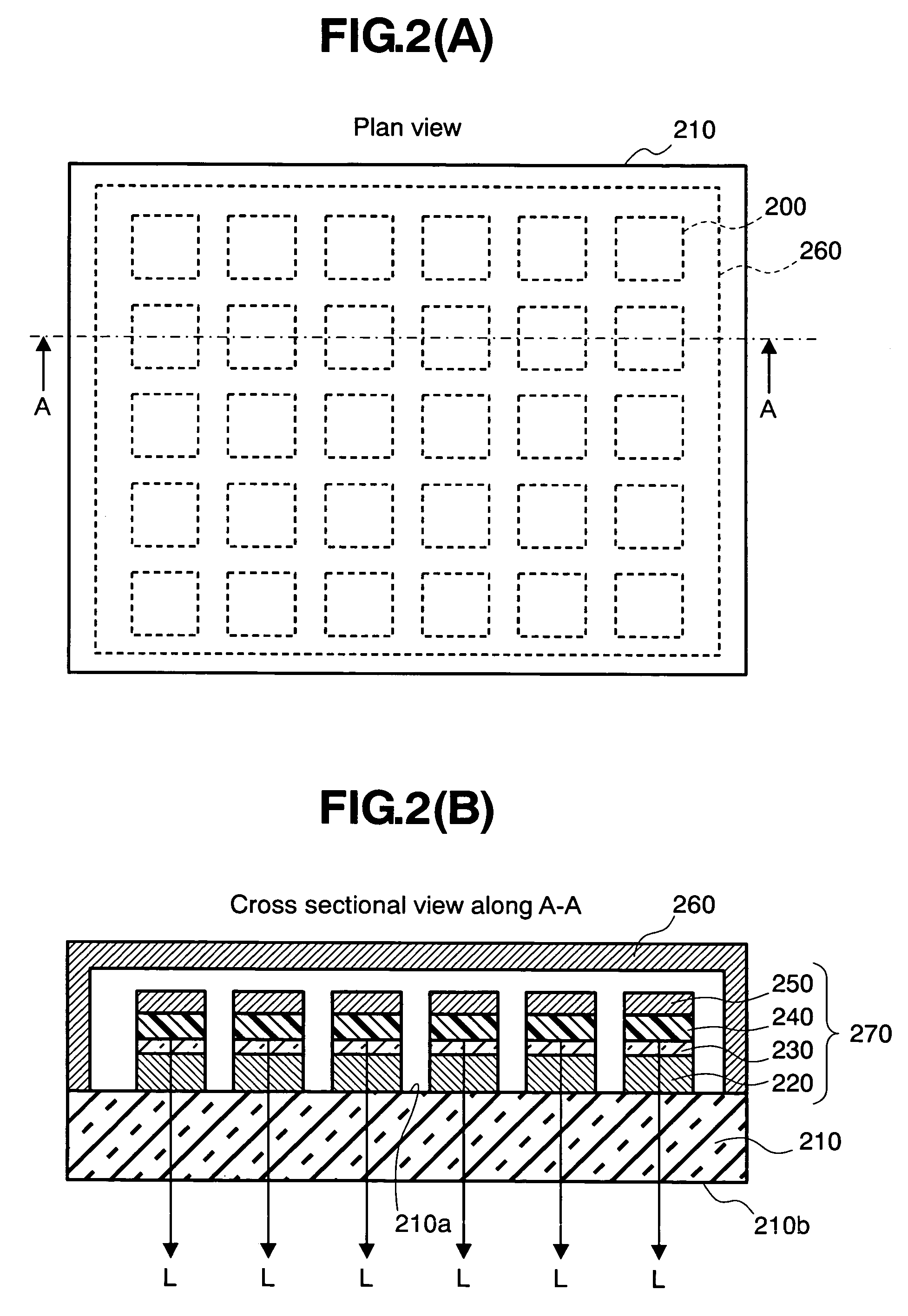
[0028]FIG. 1 is a schematic flow chart of steps for manufacturing an organic EL display according to this embodiment. FIG. 2A is a plan view of an organic EL manufactured by the manufacturing steps and FIG. 2B is a cross sectional view taken along line A-A of FIG. 2A.

[0029]At first, driving circuit layers 220 for driving pixels are formed respectively in a plurality of pixel regions 200 defined as a matrix in one surface (hereinafter referred to as rearface) 210a of a glass substrate 210 (S100). First electrodes 230 optically transparent in a visible light region are respectively deposited on the driving circuit layers 220 (S110).

[003...


PUM


Abstract

When any of pixels is not lit in an organic EL display having an organic EL layer between a first electrode and a second electrode, an organic layer of the pixel is observed. If the organic layer of the pixel contains foreign matter, the second electrode is separated into a region in contact with the foreign matter and a region not in contact with both the contact region and the foreign matter. Thus, not-lit display regions are reduced as less as possible, making it possible to manufacture an organic EL display excellent in display performance.

Description

BACKGROUND OF THE INVENTION[0001]The present invention relates to a technique for manufacturing an organic electroluminescence (EL) display and, more in particular, it relates to a method for manufacturing an organic electroluminescence display excellent in display performance with efficiency.[0002]If foreign matter is contained in an organic light emission layer of an organic EL device, defective pixels (pixels of defective emission, pixels with no emission, etc.), sometimes occur due to short-circuit between electrodes (metal electrodes, transparent electrodes) sandwiching the organic light emission layer. Techniques described in Patent Documents 1 and 2 have been known as a technique for restoring such defective pixels.[0003]According to the technique described in Patent Document 1, a region causing shortcircuit or the like is removed by laser from metal electrodes corresponding to a defective pixel. Since this enables the organic light emission layer between a partially removed ...

Claims


Application Information

Patent Timeline
Patent Type & Authority Patents(United States)
IPC IPC(8): H01J9/00H05B33/10G09F9/30H01L51/50H05B33/12H05B33/14H05B33/22H05B33/26
CPCH01L51/56H01L2251/568H10K71/861H10K71/00H10K71/70
Inventor TAMURA, TAKUOHONGO, MIKIOOKUNAKA, MASAAKIKATO, SHINICHIMATSUZAKI, EIJIITO, MASATOTERAKADO, MASATOMO
Owner SAMSUNG DISPLAY CO LTD
Why Eureka
Try Eureka