Circular test pads on scribe street area

a technology of test pads and scribe streets, which is applied in the direction of individual semiconductor device testing, semiconductor/solid-state device testing/measurement, instruments, etc., can solve the problems of increasing problems, reducing the overall yield of dies which can be fabricated from wafers, and damaged circuitry, so as to reduce reliability risks, increase wafer yield, and reduce yield loss at the wafer saw

Inactive Publication Date: 2007-08-21
TEXAS INSTR INC
View PDF43 Cites 6 Cited by
  • Summary
  • Abstract
  • Description
  • Claims
  • Application Information

AI Technical Summary

Benefits of technology

[0008]The present invention achieves technical advantages as a wafer design and process utilizing circular test pads on the scribe street such that any cracks generated in the circular test pad self terminate along the edge of the circular test pad, thereby increasing wafer yield.
[0009]According to the present invention, the test pads are designed to have a curved profile, and preferably a round periphery. Advantageously, as this round test pad is cut during wafer saw, the cracks will not extend from a sharp corner into the active die, such as is typical with the square test pads conventionally provided. Advantageously, this solution is stra...

Problems solved by technology

Accordingly, even slight propagation of cracks in the scribe street formed during the wafer saw process eventually results in damaged circuitry since the design of conventional test pads does not prevent them from extending into the active circuitry area 12, as depicted in FIG. 2.
These cracks render the particular die 1...

Method used


Image

  • Circular test pads on scribe street area
  • Circular test pads on scribe street area
  • Circular test pads on scribe street area

Examples


Embodiment Construction

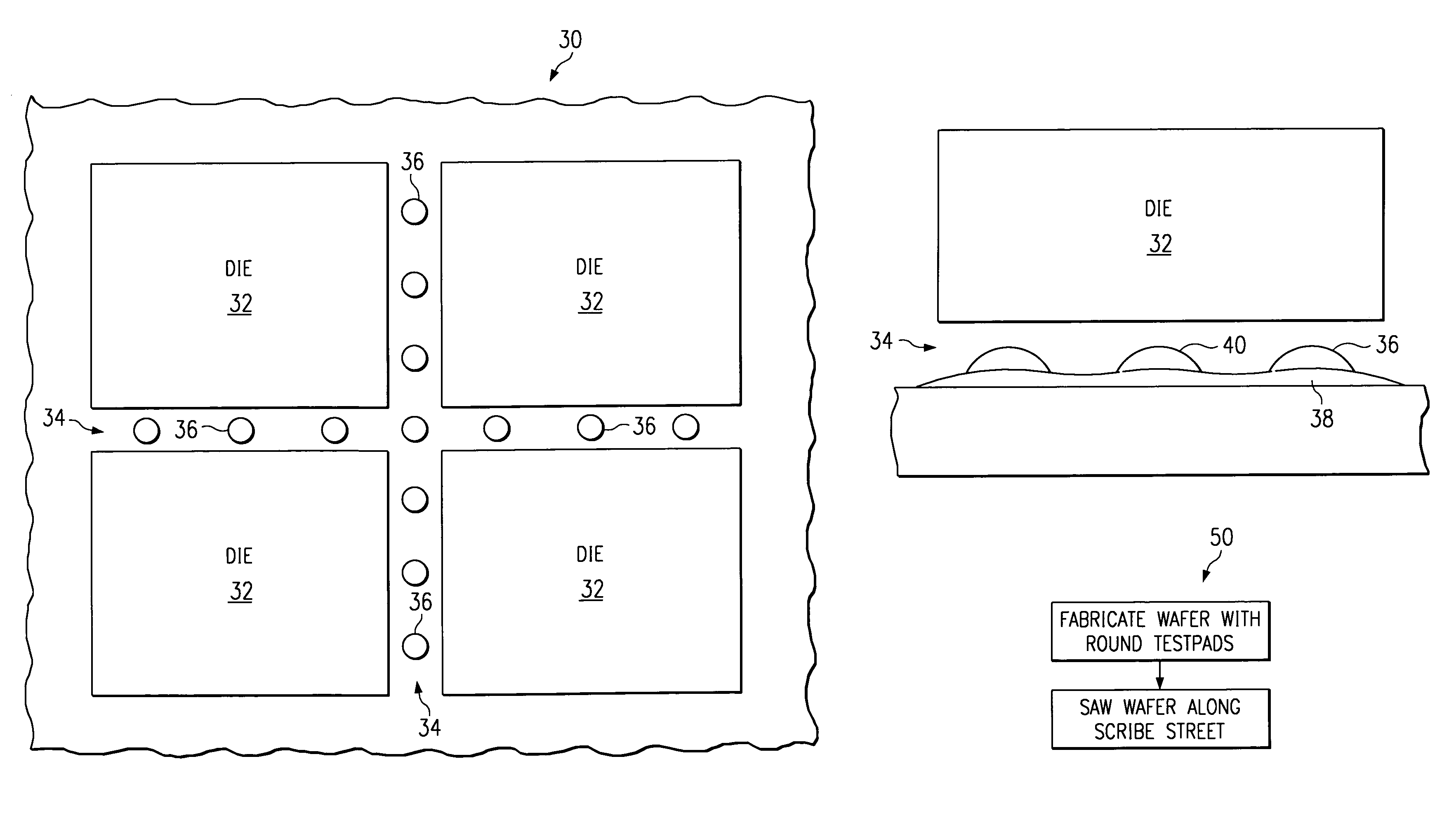
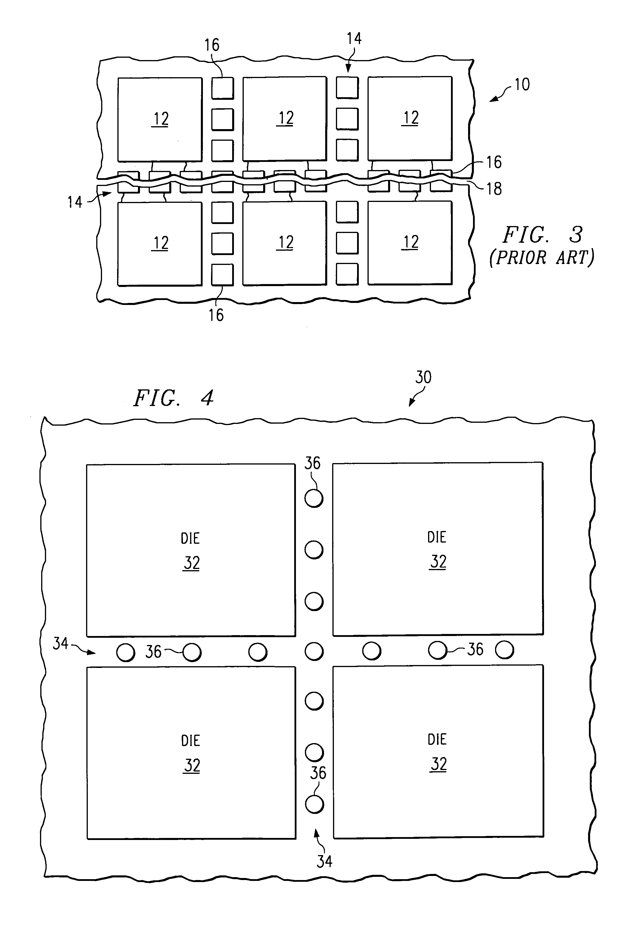
[0017]Referring now to FIG. 4, there is depicted at 30 a semiconductor wafer having a plurality of active circuits 32 (die) being formed upon the semiconductor wafer according to conventional semiconductor wafer fab processing. Defined in two dimensions between each of the formed die 32 are elongated scribe streets, generally shown at 34. Scribe streets 34 provide physical and electrical separation between the die 32, and are later cut using a wafer saw process to separate the active die for subsequent packaging.

[0018]Advantageously, as shown in FIG. 4, a plurality of test pads 36 are provided in the scribe street area 34 which have the curved profile, preferably shown as having a round periphery, as shown, but which could have other curved peripheries, such as oval or elliptical. Each of these test pads is electrically connected to one or more of the adjacent die 32, and provide a suitable electrical connection point for test equipment (not shown) to electrically test and operate t...


PUM


Abstract

A semiconductor wafer design and process having test pads (36) reducing cracks generated during the wafer saw process from extending into and damaging adjacent die. The present invention provides a plurality of circular test pads (36) in a wafer scribe street (34) such that any cracks generated in the test pad during wafer saw self terminate in the periphery of the circular test pad. By providing a curved test pad periphery, cracks will tend to propagate along the edges of the test pads and self terminate therein. The circular test pads avoid any sharp corners as is conventional in rectangular test pads which tend to facilitate the extension of cracks from corners to extend into the adjacent wafer die (32). The present invention utilizes existing semiconductor fab processing and utilizes new reticle sets to define the curved test pads.

Description

FIELD OF THE INVENTION[0001]The present invention is generally related to semiconductor wafer processing, and more particularly to scribe streets extending between formed active areas and test pads located thereon for testing the active devices.BACKGROUND OF THE INVENTION[0002]Integrated circuits are typically defined on a semiconductor wafer using a variety of wafer fab processes. Each of the formed active circuit areas, later forming integrated circuits after dicing and packaging, are physically separated from one another on the wafer by an elongated region commonly referred to as a scribe street. These wafers are typically cut along the scribe street after circuit testing using a conventional saw process.[0003]In addition to the active circuitry formed on the semiconductor wafer, test pads are also provided to facilitate the active testing of the formed circuitry prior to the wafer saw process. Typically, these test pads are formed in the scribe streets, and are cut away during t...

Claims


Application Information

Patent Timeline
IPC IPC(8): H01L21/00H01L23/58
CPCH01L22/32
Inventor ROLDA, JR., RUBEN A.VALERIO, RICHARDOLERO, JENNY
Owner TEXAS INSTR INC
Why Eureka
Try Eureka