N-level down hierarchical powergrid analysis

a powergrid and hierarchical analysis technology, applied in the field of performing powergrid analysis, can solve the problems of inability to accurately locate the ports between local and global powergrids, inability to include every circuit element in a full powergrid analysis, and adverse effects on the overall circuit design. the effect of global powergrid analysis

Active Publication Date: 2007-08-21
ORACLE INT CORP
View PDF2 Cites 0 Cited by
  • Summary
  • Abstract
  • Description
  • Claims
  • Application Information

AI Technical Summary

Benefits of technology

[0010]As used herein, the term “local cell” refers generally to a portion of a semiconductor circuit that is modeled as a unit, independent of other portions of the semiconductor circuit. Such an independent circuit portion may include a library cell, a block, a metacell, etc. A “local powergrid” refers, generally, to a collection of metal layers serving a local c

Problems solved by technology

Many of these semiconductor devices, however, have so many circuit elements that including every circuit element in a full powergrid analysis can be impractical.
A drawback of some conventional hierarchical analysis techniques is that if a designer performs a global powergrid analysis during earlier stages of the design cycle,

Method used


Image

  • N-level down hierarchical powergrid analysis
  • N-level down hierarchical powergrid analysis
  • N-level down hierarchical powergrid analysis

Examples


Embodiment Construction

)

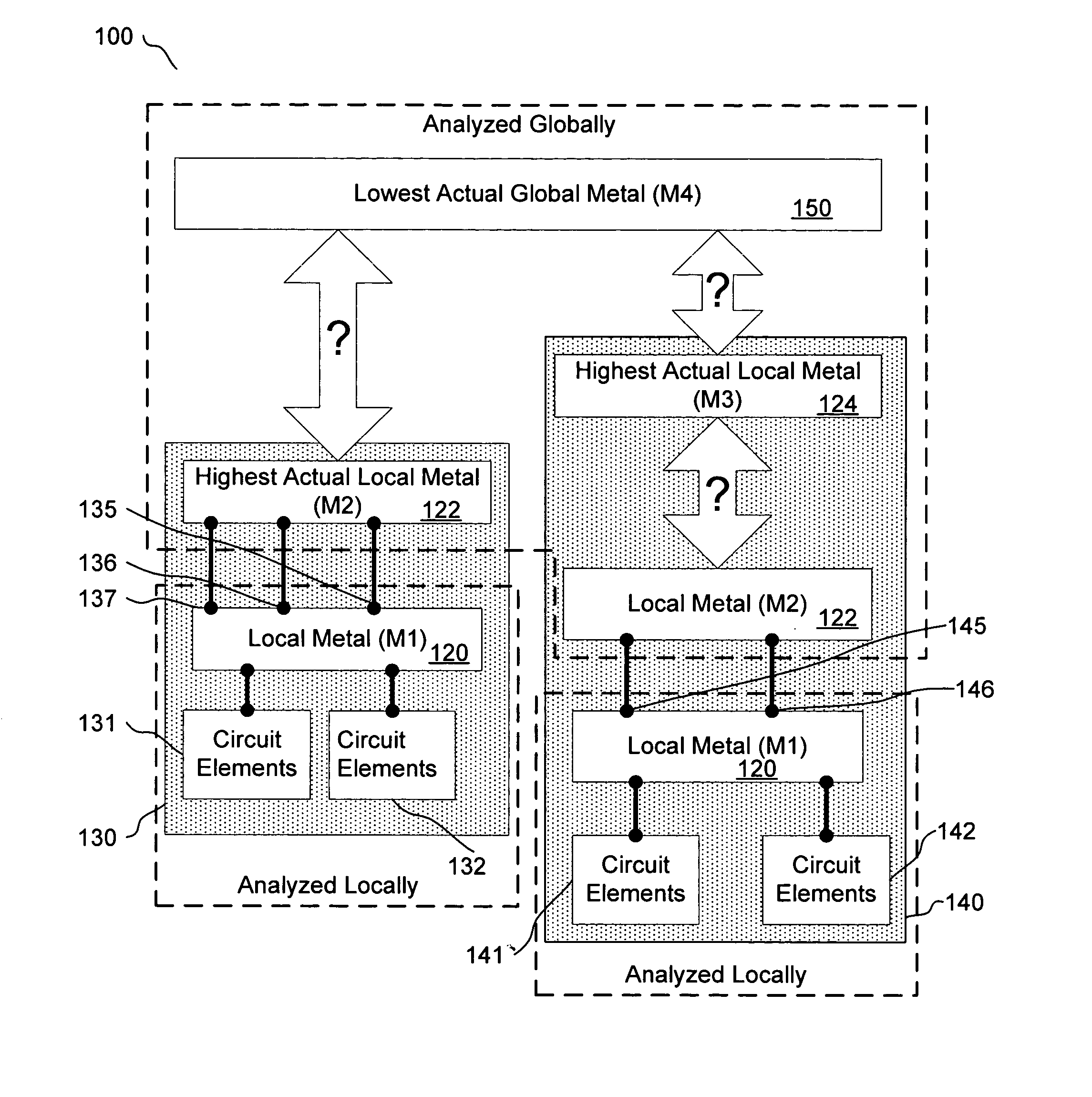
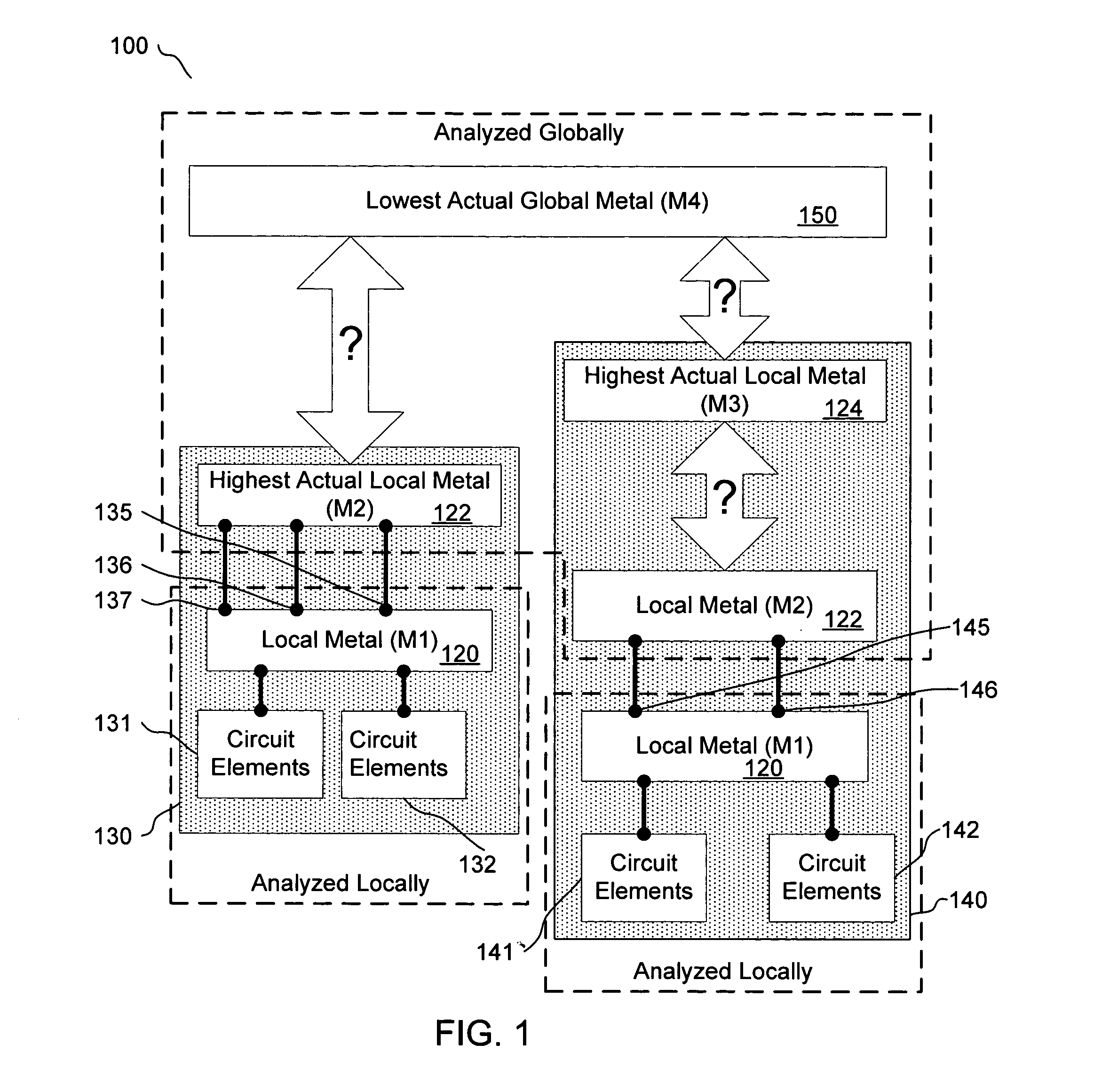
[0020]Referring first to FIG. 1, techniques for grouping power grids for hierarchical analysis will be discussed according to an embodiment of the present invention. As known to those skilled in the art, semiconductor structures such as transistors, capacitors, diodes, and the like are often placed on a semiconductor substrate so that functionally related structures are located close to each other. These groups of functionally related semiconductor structures, or circuit elements, are sometimes referred to as cells.

[0021]The circuit elements within cells are usually interconnected by one or more metal layers, which are used to route signals and power to individual circuit elements. The metal layers used to interconnect circuit elements internal to a cell are commonly referred to as local power grids. It should be noted, however, that the term “local power grid” sometimes includes not only the interconnecting metal layers, but also the circuit elements connected by the metal layers....


PUM


Abstract

Ports at which a cell served by a local powergrid is to be modeled are designated on a selected metal layer N-levels down from the topmost metal layer of the local powergrid. The cell is modeled at the designated ports, excluding any metal layers above the selected metal layer. Any metal layers of the local powergrid above the selected metal layer are included as part of a model of the global powergrid, rather than as part of the local powergrid, and a hierarchical powergrid analysis is performed.

Description

CROSS-REFERENCE TO RELATED APPLICATION(S)[0001]This application is related to application Ser. No. 10 / 876,218, entitled, “METHOD OF MODELING CIRCUIT CELLS FOR POWERGRID ANALYSIS”, naming Xiaoning Qi, Anuj Trivedi and Kenneth Y. Yan as inventors, filed of even date and of common assignee herewith.BACKGROUND[0002]1. Field of the Invention[0003]This invention relates generally to performing powergrid analysis, and more particularly to choosing port locations for hierarchical powergrid analysis.[0004]2. Description of the Related Art[0005]Performing electromigration (EM) risk and voltage (IR) drop analyses of a full-chip powergrid are important steps in designing modern processors and other semiconductor devices. Many of these semiconductor devices, however, have so many circuit elements that including every circuit element in a full powergrid analysis can be impractical. To address this issue, circuit designers sometimes employ hierarchical powergrid analysis.[0006]In hierarchical powe...

Claims


Application Information

Patent Timeline
IPC IPC(8): G06F17/50
CPCG06F17/5036G06F30/367
Inventor YAN, KENNETH Y.TRIVEDI, ANUJQI, XIAONING
Owner ORACLE INT CORP
Why Eureka
Try Eureka