Semiconductor-mounted device and method for producing same

a semiconductor and mounting device technology, applied in the direction of semiconductor devices, semiconductor/solid-state device details, electrical apparatus, etc., can solve the problems of increased cost, increased size and thickness, and increased packaging costs, so as to achieve good industrial effect, eliminate restrictions on the constitution of semiconductor-mounted devices, and good industrial

Inactive Publication Date: 2007-08-28
RENESAS ELECTRONICS CORP
View PDF9 Cites 63 Cited by
  • Summary
  • Abstract
  • Description
  • Claims
  • Application Information

AI Technical Summary

Benefits of technology

[0011]It is an object of the present invention in a second aspect to provide a semiconductor-mounted device in which positions of mounting semiconductor chips are different between both sides of a wired board, and a producing method thereof; it does not largely increases the costs as compared with the solution of the first aspect, does not generate any problem of the reliance such as the bad connection of the projecting electrodes and the cracks or peeling of the sealing resin, and does not reduce the space around the semiconductor-mounted device.
[0020]The semiconductor-mounted device and the producing method thereof in the first aspect of the present invention can achieve a good industrial effect that a semiconductor-mounted device can be provided in which semiconductor chips can be mounted on any positions of both sides of a wired board freed of the open defect.
[0021]In the first aspect of the present invention, as shown in FIG. 1, a semiconductor-mounted device 8 comprises a sealing resin 1 covering, with a same height, a region disposed at and around a first semiconductor chip 3a mounted on a first side of a wired board and opposite, across the wired board 2, to at least an area of projecting electrodes 4 of a second semiconductor chip 3b mounted on a second side of the wired board, and a producing method thereof. Therefore, when heat and pressure are applied to the second semiconductor chip 3b, the wired board 2 just under the projecting electrodes 4 of the second semiconductor chip 3b is supported by the sealing resin 1, so the heat and pressure do not generate any warp, the electrode pads of the wired board 2 and the projecting electrodes 4 being securely connected, thereby freed from generation of open defect. The region sealed with the resin at the side of the first semiconductor chip 3a can be also modified at any time corresponding to the position at which the second semiconductor chip 3b is mounted, so that the position of the second semiconductor chip 3b can be arbitrarily selected and thus restrictions of the constitution of the semiconductor-mounted device can be eliminated.
[0022]The semiconductor-mounted devices and the producing methods thereof in the second aspect of the present invention can achieve a good industrial effect that a semiconductor-mounted device can be provided in which positions at which semiconductor chips are mounted can be different from one side to the other side of a wired board; the semiconductor-mounted device does not largely increase its costs as compared with the above-mentioned method of the resin seal, further freed from the problems of reliance such as connection error of projecting electrodes and cracks or peeling of the sealing resin, and does not largely reduce the space around the semiconductor-mounted device.

Problems solved by technology

However, there are problems that the size and thickness become larger as compared with the semiconductor chip per se, and that the packaging is costly.
The costs become greater because the wired board has to be transferred from a stage to a sealing mold, be sealed, and be placed on the stage again, and because an expensive sealing mold is necessary.
There is also probability that repetition of generating heat and cooling during working of the semiconductor chip generates a problem of reliance such as connection defect of projecting electrodes and cracks or peeling of a sealing resin because the sealing resin whose thermal expansion coefficient is largely different from that of the wired board or semiconductor chip forms an asymmetric constitution.
There is further probability that the semiconductor-mounted device interferes with other electronic devices because a first side of the wired board is covered with the sealing resin, thereby reducing an effective space for further mounting of the semiconductor-mounted device.

Method used


Image

  • Semiconductor-mounted device and method for producing same
  • Semiconductor-mounted device and method for producing same
  • Semiconductor-mounted device and method for producing same

Examples


Embodiment Construction

[0036]Embodiments of the present invention will be explained below referring to the attached drawings, in which the symbols coincide with ones of the same matter as the conventional art.

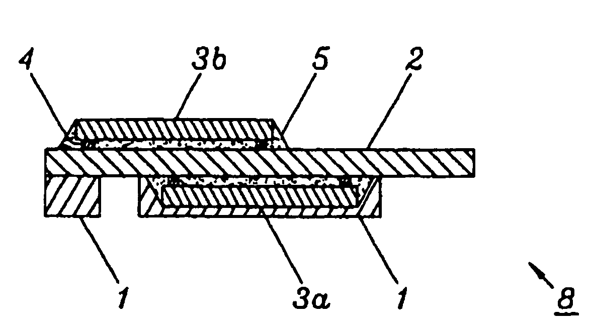
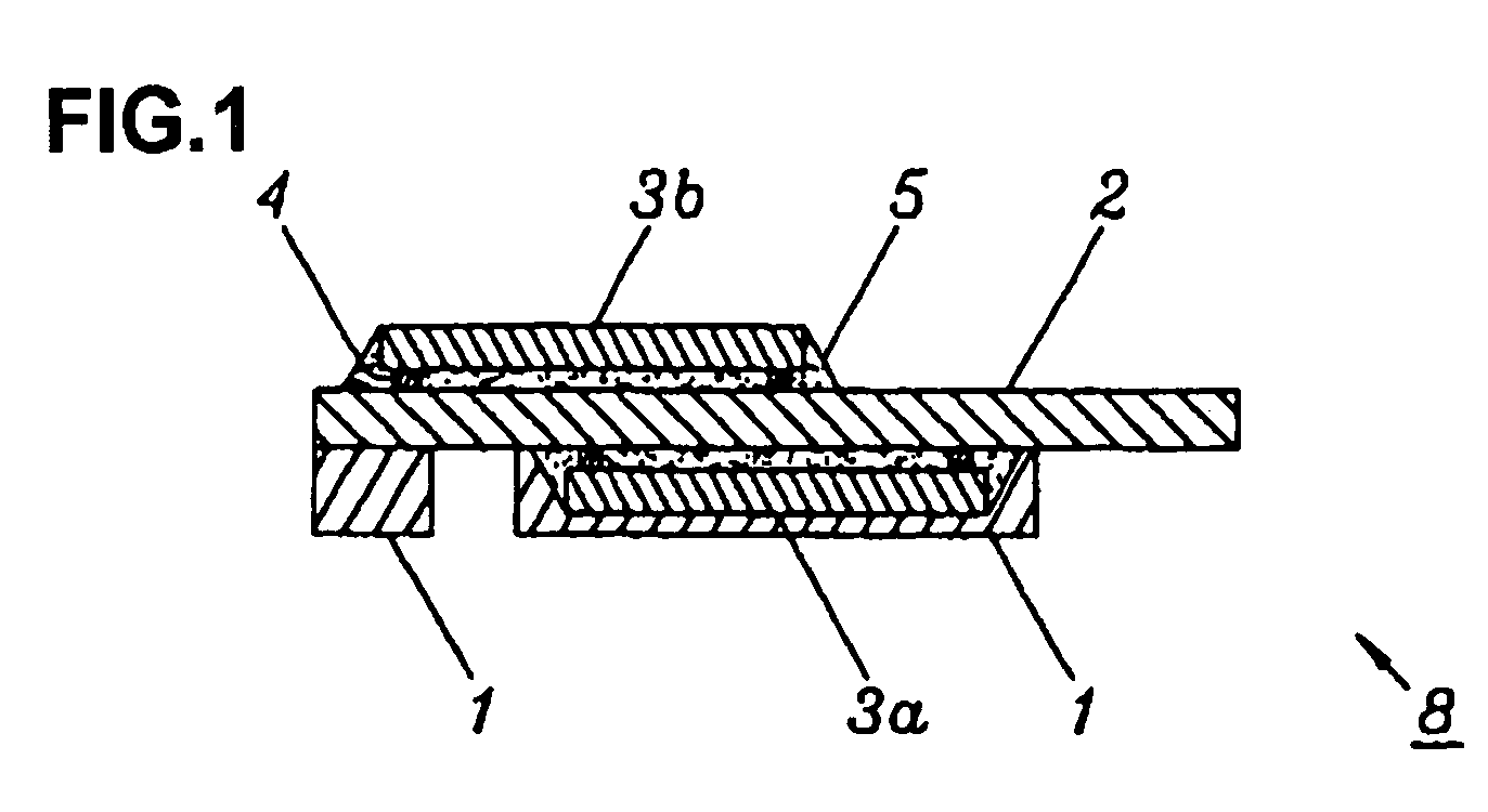
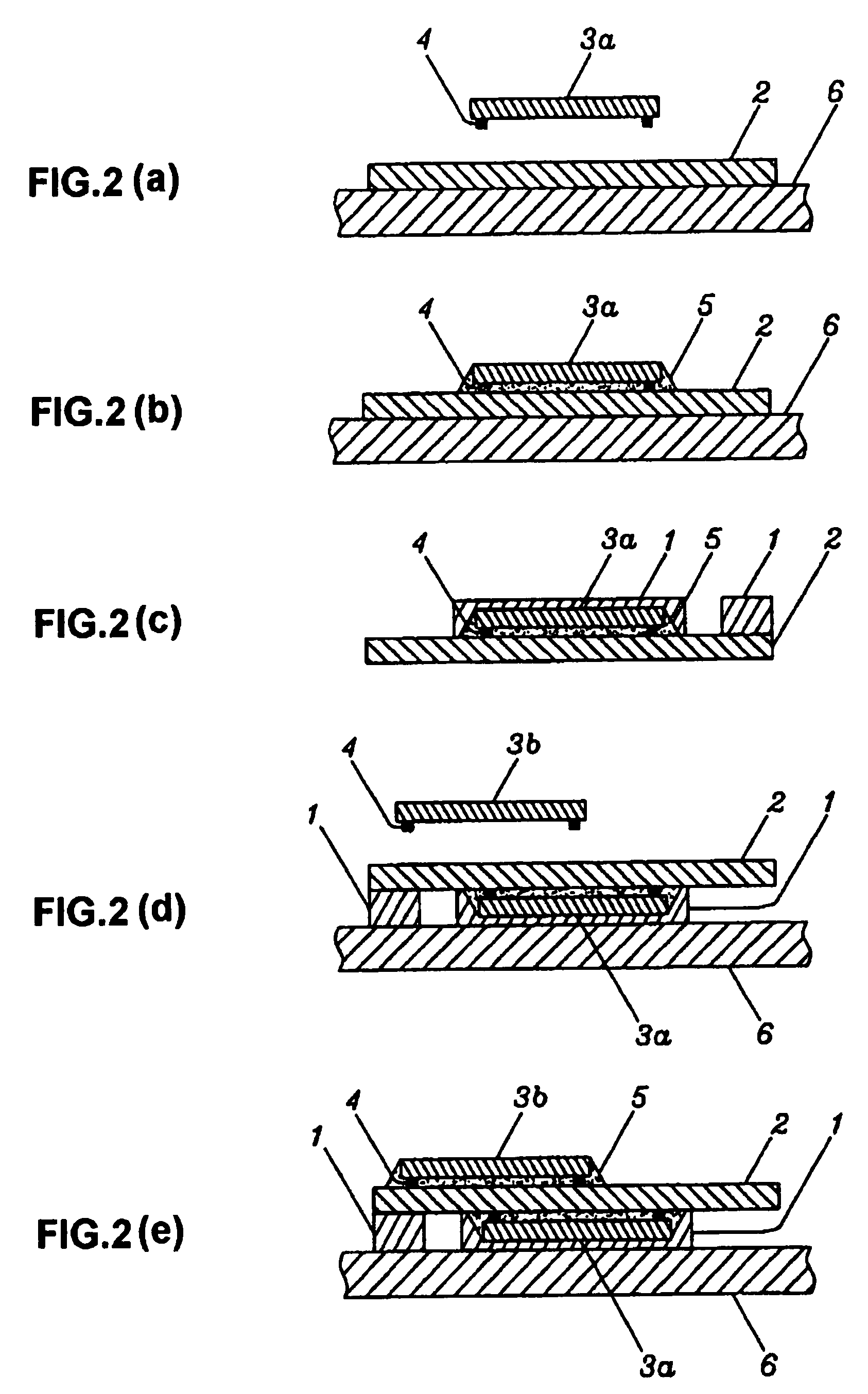
[0037]According to a first aspect of the present invention, as shown in FIG. 1, in a semiconductor-mounted device of an embodiment of the present invention, electrode pads (not shown) of a wired board 2 and projecting electrodes 4 of semiconductor chips 3a, 3b are electrically and mechanically connected on both sides of the wired board 2, the wired board 2 and the semiconductor chips 3a, 3b being adhered by an underfill resin 5. The semiconductor-mounted device 8 of the present invention comprises a sealing resin 1 which seals a region disposed at and around the first semiconductor chip 3a mounted on the first side of the wired board and at the position opposite, across the wired board, to at least an area of the projecting electrodes 4 of the second semiconductor chip 3b mounted on the second side o...


PUM


Abstract

Semiconductor-mounted device comprises wired board, first semiconductor chip mounted on first side of wired board, second semiconductor chip mounted on second side of wired board and sealing resin sealing, with a same height, a region disposed at and around first semiconductor chip and opposite, across wired board, to at least an area of projecting electrodes of second semiconductor chip; and a producing method thereof. Semiconductor-mounted device also comprises wired board, first semiconductor chip mounted on first side of wired board, second semiconductor chip mounted on second side of wired board and resin sheet covering, at substantially a same height as first semiconductor chip, a region disposed around first semiconductor chip and opposite, across wired board, to at least an area of projecting electrodes of second semiconductor chip, back surface of first semiconductor chip being exposed; and a producing method thereof.

Description

FIELD OF THE INVENTION[0001]The present invention relates to a semiconductor-mounted device mounted semiconductor chips on both sides of a wired board and a producing method thereof, particularly, a semiconductor-mounted device in which a semiconductor chip of a front side of a wired board is not aligned with a semiconductor chip of a back side of a wired board and a producing method thereof.BACKGROUND OF THE INVENTION[0002]In order to meet a requirement for miniaturizing and thinning an electronic device, a method has been adopted that finely miniaturizes a semiconductor chip pattern, and that mounts semiconductor chips on both sides of a wired board, thereby increasing a mounting efficiency.[0003]An example of a semiconductor-mounted device mounted with semiconductor chips on both sides of a wired board is shown in FIG. 10. Electrode pads (not shown) of a wired board 2 and projecting electrodes 4 of a semiconductor chip 3 are electrically and mechanically connected at opposite pos...

Claims


Application Information

Patent Timeline
Patent Type & Authority Patents(United States)
IPC IPC(8): H01L23/48H01L23/52H01L29/40H01L21/50H01L21/60H01L23/02H01L23/12H01L23/28H01L25/04H01L25/065H01L25/18
CPCH01L25/0657H01L2225/06517H01L2225/06582H01L2225/06589H01L2225/06593H01L2924/01078H01L2224/16225H01L2924/18161H01L2224/73204H01L2224/32225H01L2924/00012
Inventor HINO, SHIGEKAZUMAGOI, TAKASHIIWANAGA, SYUNICHI
Owner RENESAS ELECTRONICS CORP
Why Eureka
Try Eureka