

3-d stacking of active devices over passive devices
a technology of active devices and passive devices, applied in the direction of printed circuits, sustainable manufacturing/processing, final product manufacturing, etc., can solve the problems of undesirable use high manufacturing cost and time-consuming of integrated passive devices, etc., to reduce the space required by passive devices, increase the density of boards, and reduce the size of substrates
- Summary
- Abstract
- Description
- Claims
- Application Information
AI Technical Summary
Benefits of technology
Problems solved by technology
Method used
Image

Examples
Embodiment Construction
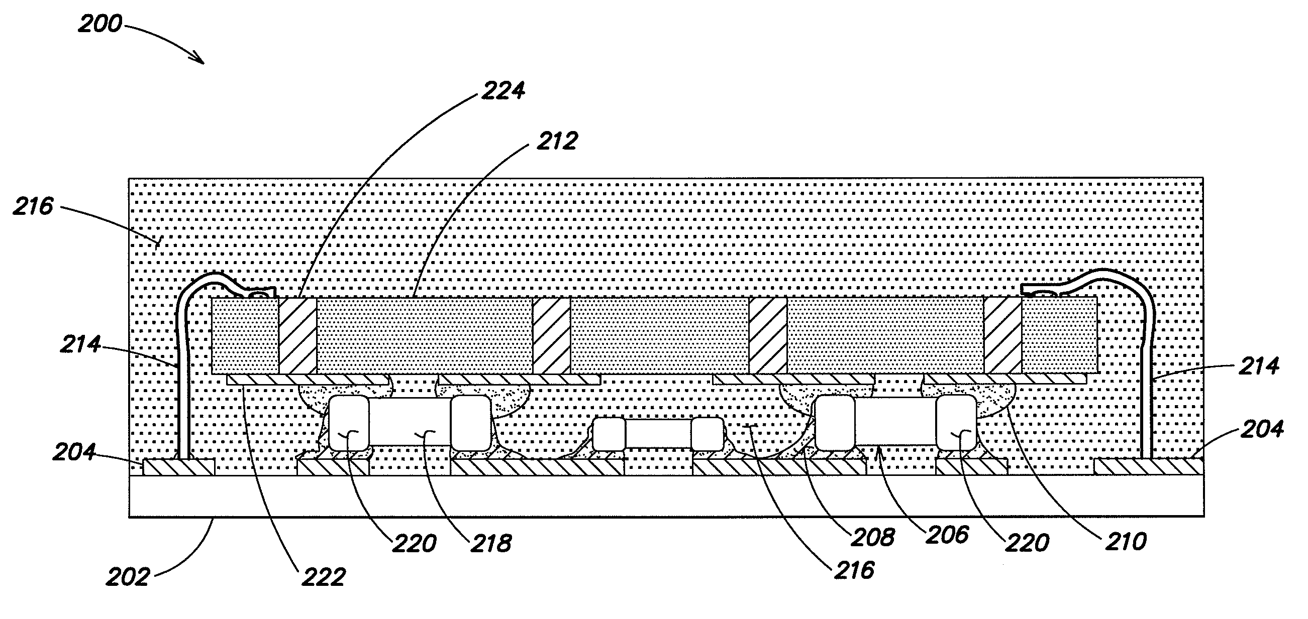
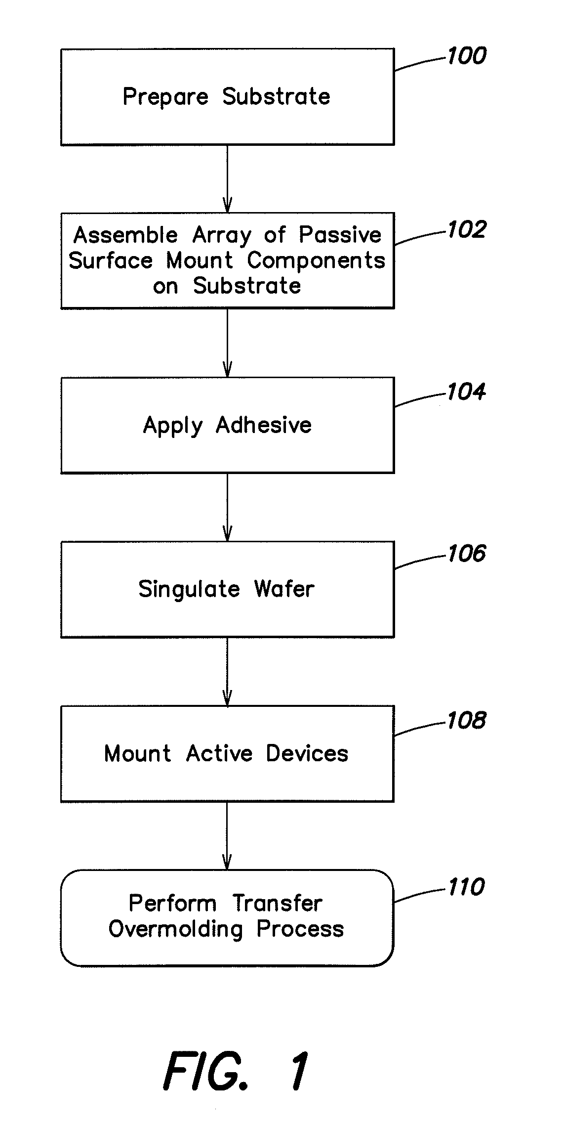
[0019]As discussed above, in order to accommodate the growing demand for smaller and more complex electronic devices, designers have moved toward electronic modules that incorporate vertically stacked devices in a three-dimensional (3-D) geometry. Conventionally, for 3-D modules that comprise many passive devices, the tendency has been to stack active integrated circuits (ICs) over integrated passive devices. These integrated passive devices are formed using semiconductor fabrication technologies (e.g., silicon-on-insulator technology, thin-film technology, etc.) and are incorporated into the module during die fabrication and assembly, which typically occurs in a clean room environment.
[0020]Although the use of integrated passive devices allows some increase in the effective surface area of the substrate board (by enabling vertical stacking of active ICs above the integrated passive devices), there are several disadvantages associated with it. For example, integrated passive devices...
PUM
 Abstract
Description
Claims
Application Information