
Memory circuit with flexible bitline-related and/or wordline-related defect memory cell substitution

a memory cell and defect technology, applied in the field of memory circuits, can solve the problems of increasing the yield of substitution memory cells, unusable ram circuits with defect memory cells, and increasing the memory access time of ram circuits, so as to reduce the overhead of memory redundancy and less densely packed

Inactive Publication Date: 2007-08-28
LONGITUDE LICENSING LTD
View PDF11 Cites 8 Cited by
  • Summary
  • Abstract
  • Description
  • Claims
  • Application Information

AI Technical Summary

Benefits of technology

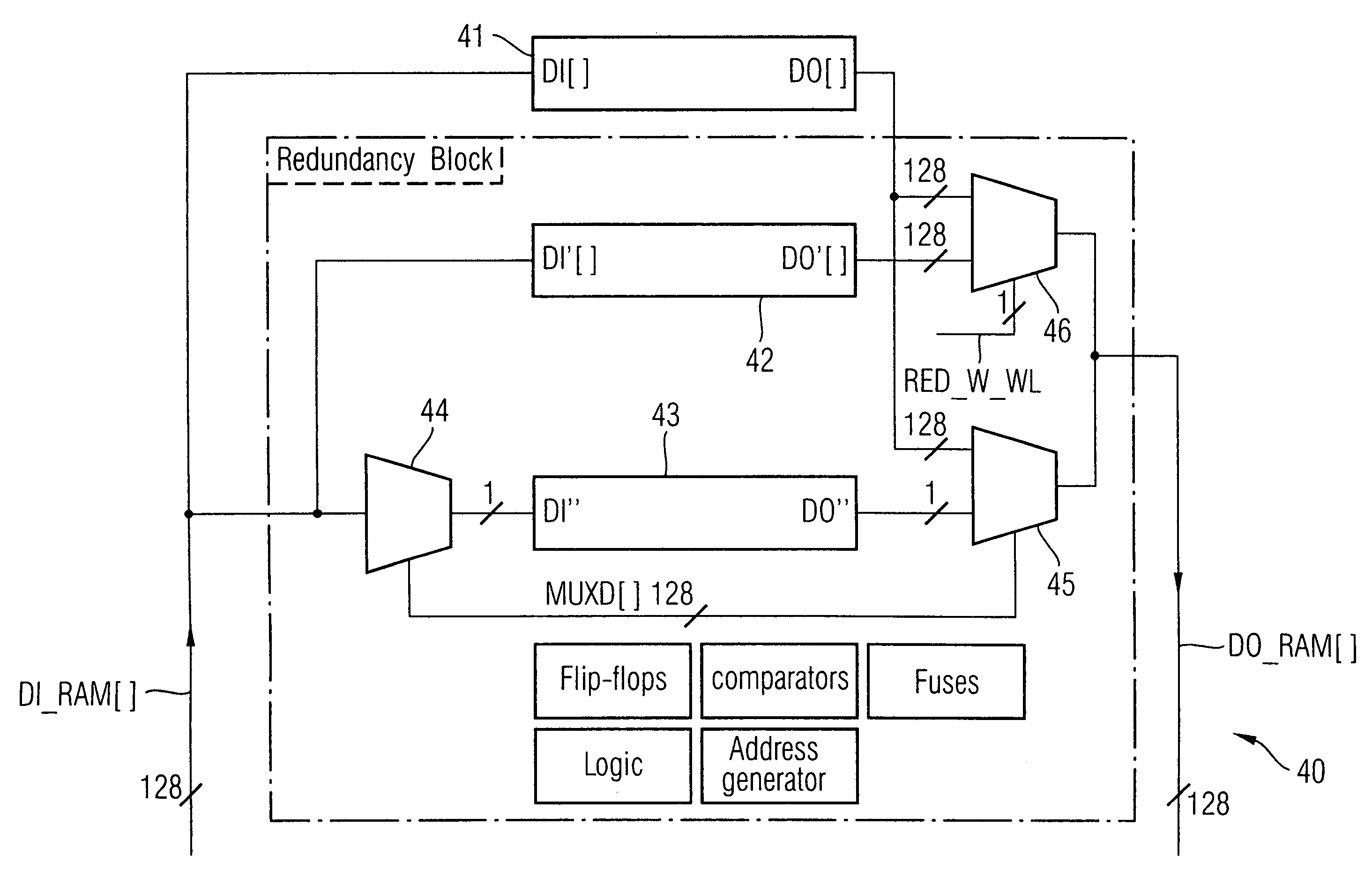
[0033]The inventive external bitline-related repair approach provides the advantage that the physical implementation of the substitution memory block is not bound to the physical implementation of the main memory block. Advantageously, the substitution memory cells within the substitution memory block are less densely packed compared to the memory cells within the main memory block.
[0034]A further advantage of the memory circuit is that the processing speed of the circuit is generally not affected by the memory redundancy since the comparison can be performed in parallel to the main memory access.
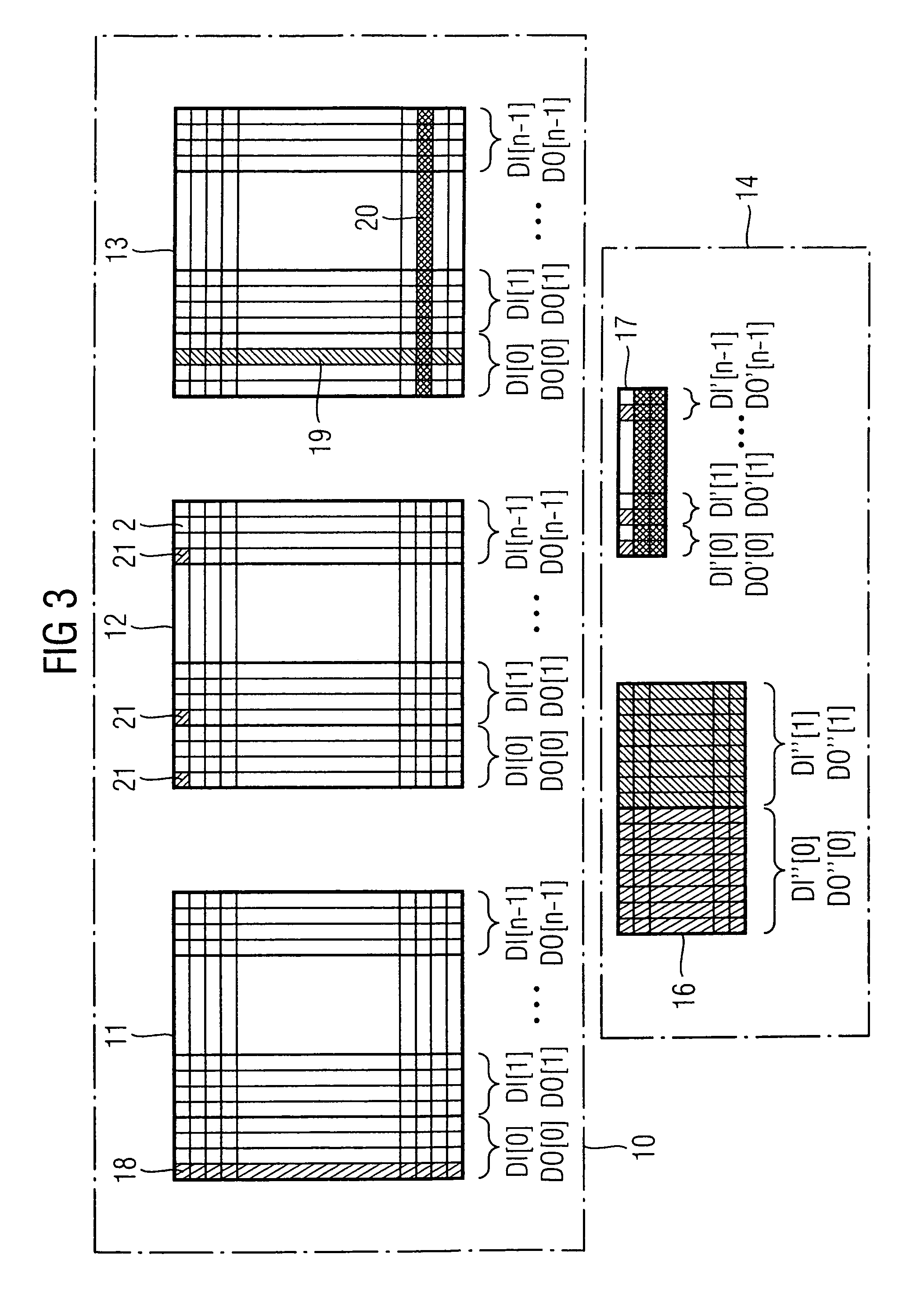
[0035]In addition, the inventive solution provides the option that the substitution memory block can be shared for the substitution of several memory arrays within the main memory block. Thus, the total area overhead due to memory redundancy is reduced.
[0086]Regarding the first or alternatively the second aspect of the invention, the substitution memory cells within the substitution memory block are advantageously less dense packed compared to the memory cells within the main memory block, i.e. larger substitution memory cells in comparison to the memory cells of the main memory are used, resulting in an increased yield regarding the substitution memory block. Thus, the design rules of a semiconductor technology, which limit the physical dimensions on the lower end, can be followed within the substitution memory block. Layout waivers, which break these rules in favor of a denser layout and which are critical for the fabrication of the memory circuit, are not necessary for the substitution memory block. Furthermore, the increased physical dimensions of the substitution memory cells enable flexible usage of the substitution memory block for process technologies with smaller as well as larger feature sizes.

Problems solved by technology

Without appropriate countermeasures such RAM circuits with defect memory cells would be unusable for most applications even if only a small number of memory cells compared to the total number is affected.
Thus, process failures affecting the yield of the memory cells of the main memory affect the yield of the substitution memory cells in the same way.
A further drawback of such an implementation of the bitline-related repair approach or alternatively the wordline-related repair is that the memory access time of the RAM circuit is increased in comparison to the memory access time of a RAM circuit without bitline-related or wordline-related substitution memory.
This leads to a large area over-head.
In addition, the concrete implementation of the bitline-related or wordline-related repair approach is only valid for a particular implementation of the main memory.
The substitution memory is not capable to substitute complete wordline-related sets of memory cells or bitline-related sets of memory cells.

Method used


Image

  • Memory circuit with flexible bitline-related and/or wordline-related defect memory cell substitution
  • Memory circuit with flexible bitline-related and/or wordline-related defect memory cell substitution
  • Memory circuit with flexible bitline-related and/or wordline-related defect memory cell substitution

Examples


Embodiment Construction

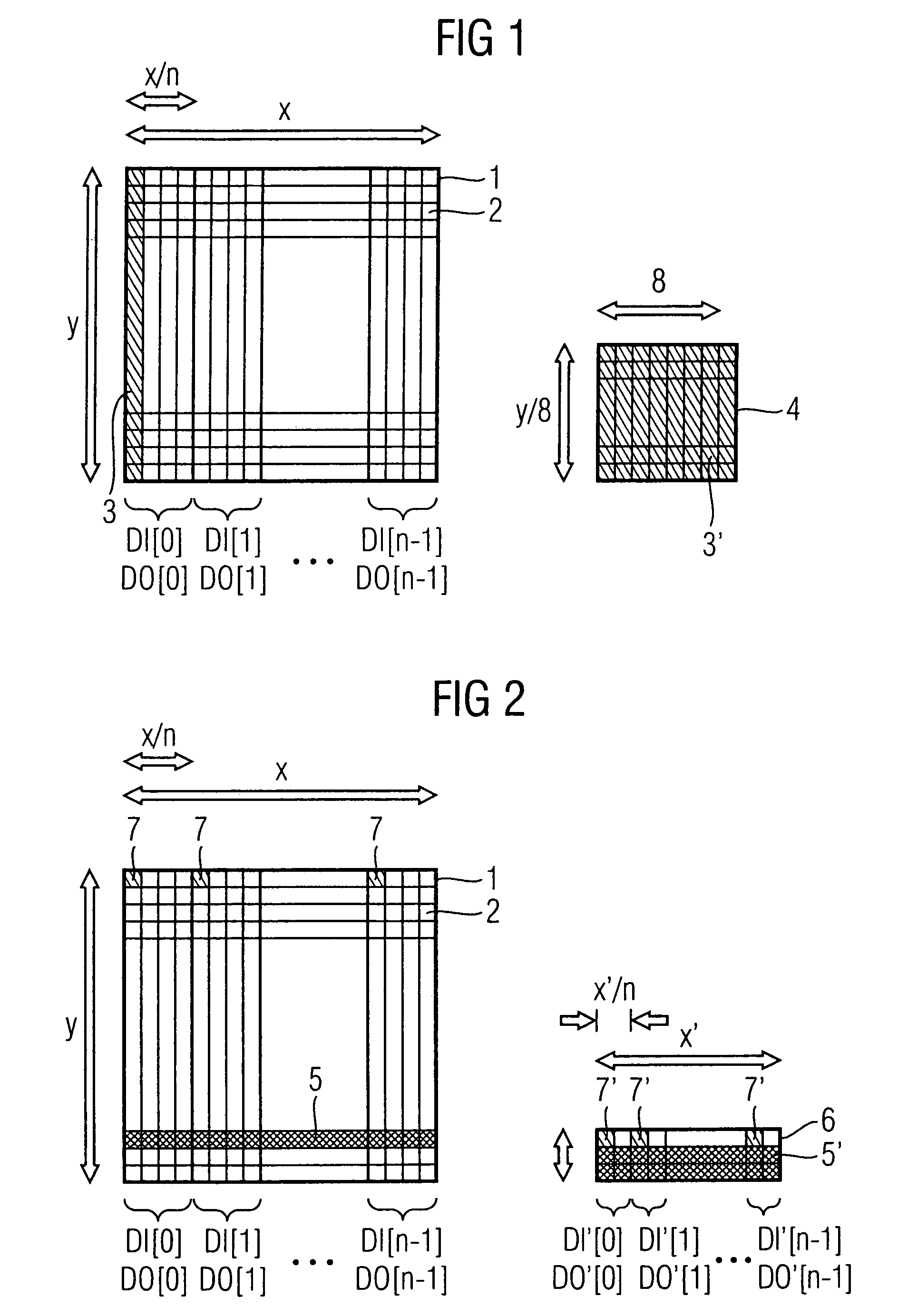
[0094]FIG. 1 gives a basic illustration of an inventive RAM circuit based on the inventive external bitline-related repair approach. The memory cells 2 of a memory array 1 within a RAM circuit are arranged into y (e.g. 512) rows and x (e.g. 512) columns; the memory array 1 comprises a number of x*y memory cells 2. A plurality of x memory cells 2 within one row are assigned to one wordline (not shown), whereas a plurality of y memory cells 2 within one column are assigned to one bitline (not shown).

[0095]The memory array 1 is word-wise accessed, i.e. it comprises an n-bit-wide input and output (e.g. n=128) with n ports DI[0], DI[1], . . . DI[n−1] and DO[0], DO[1], . . . DO[n−1], respectively. To each input or output port a plurality of x / n bitlines is assigned. The selection of one bitline for each plurality of x / n bitlines is carried out by column multiplexers (not shown).

[0096]In case one or more memory cells within a particular bitline-related set 3 of memory cells 2 are defective...


PUM


Abstract

The inventive memory circuit comprises a main memory block and a substitution memory block for substitution of defect memory cells, with the substitution memory block being external to the main memory block. The substitution memory block is arranged to substitute at least one bitline-related or wordline-related set of memory cells being connected to the same bitline or wordline, respectively. Furthermore, the inventive memory circuit comprises redirection means for redirecting the access to a memory cell of the at least one respective substituted set of memory cells to the substitution memory block.

Description

CROSS-REFERENCE TO RELATED APPLICATIONS[0001]This application claims foreign priority benefits under 35 U.S.C. §119 to co-pending German patent application number EP 04 023 959.2, filed 7 Oct. 2004. This related patent application is herein incorporated by reference in its entirety.BACKGROUND OF THE INVENTION[0002]1. Field of the Invention[0003]The invention relates to memory circuits, particularly to RAM (random access memory) circuits, with memory redundancy for the substitution of defect memory cells.[0004]2. Description of the Related Art[0005]RAM circuits comprise one or more two-dimensional arrays of 1-bit-memory cells. In DRAM (dynamic random access memory) circuits the information storage in a memory cell is based on the charge state of a capacitor, whereas in SRAM (static random access memory) circuits flip-flops with positive feedback for information storage are employed.[0006]The memory cells of one array are arranged into y rows and x columns. The memory cells of one row...

Claims


Application Information

Patent Timeline
Patent Type & Authority Patents(United States)
IPC IPC(8): G11C7/00
CPCG11C29/808
Inventor GOUIN, VINCENTHIREL, LINDAPALAU, LUC
Owner LONGITUDE LICENSING LTD
Learn More