
Memory circuit with flexible bitline-related and/or wordline-related defect memory cell substitution
a memory cell and defect technology, applied in the field of memory circuits, can solve the problems of increasing the yield of substitution memory cells, unusable ram circuits with defect memory cells, and increasing the memory access time of ram circuits, so as to reduce the overhead of memory redundancy and less densely packed
Patent Information
- Authority / Receiving Office
- US · United States
- Current Assignee / Owner
- Publication Date
- 2006-04-27
- Estimated Expiration
- Not applicable · inactive patent
Smart Images
Figure 1 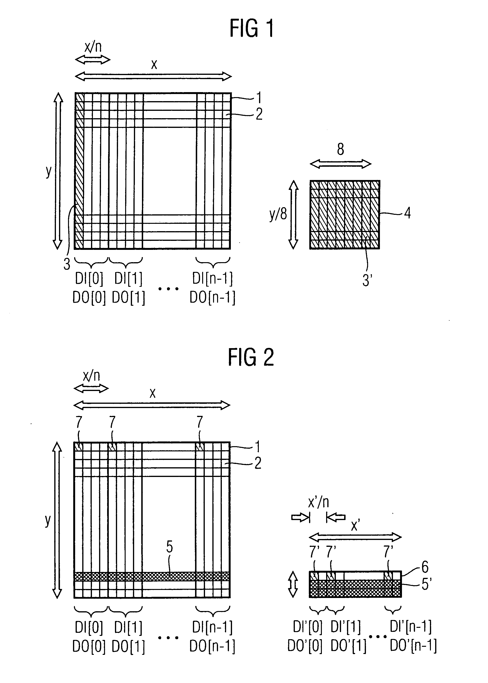
Figure 2 
Figure 3
Abstract
Description
CROSS-REFERENCE TO RELATED APPLICATIONS
[0001] This application claims foreign priority benefits under 35 U.S.C. §119 to co-pending German patent application number EP 04 023 959.2, filed 7 Oct. 2004. This related patent application is herein incorporated by reference in its entirety. BACKGROUND OF THE INVENTION
[0002] 1. Field of the Invention
[0003] The invention relates to memory circuits, particularly to RAM (random access memory) circuits, with memory redundancy for the substitution of defect memory cells.
[0004] 2. Description of the Related Art
[0005] RAM circuits comprise one or more two-dimensional arrays of 1-bit-memory cells. In DRAM (dynamic random access memory) circuits the information storage in a memory cell is based on the charge state of a capacitor, whereas in SRAM (static random access memory) circuits flip-flops with positive feedback for information storage are employed.
[0006] The memory cells of one array are arranged into y rows and x columns. The memory cel...
Examples
Embodiment Construction
[0094]FIG. 1 gives a basic illustration of an inventive RAM circuit based on the inventive external bitline-related repair approach. The memory cells 2 of a memory array 1 within a RAM circuit are arranged into y (e.g. 512) rows and x (e.g. 512) columns; the memory array 1 comprises a number of x*y memory cells 2. A plurality of x memory cells 2 within one row are assigned to one wordline (not shown), whereas a plurality of y memory cells 2 within one column are assigned to one bitline (not shown).
[0095] The memory array 1 is word-wise accessed, i.e. it comprises an n-bit-wide input and output (e.g. n=128) with n ports DI[0], DI[1], . . . DI[n−1] and DO[0], DO[1], . . . DO[n−1], respectively. To each input or output port a plurality of x / n bitlines is assigned. The selection of one bitline for each plurality of x / n bitlines is carried out by column multiplexers (not shown).
[0096] In case one or more memory cells within a particular bitline-related set 3 of memory cells 2 are defec...