Image pickup apparatus
- Summary
- Abstract
- Description
- Claims
- Application Information
AI Technical Summary
Benefits of technology
Problems solved by technology
Method used
Image
Examples
first embodiment
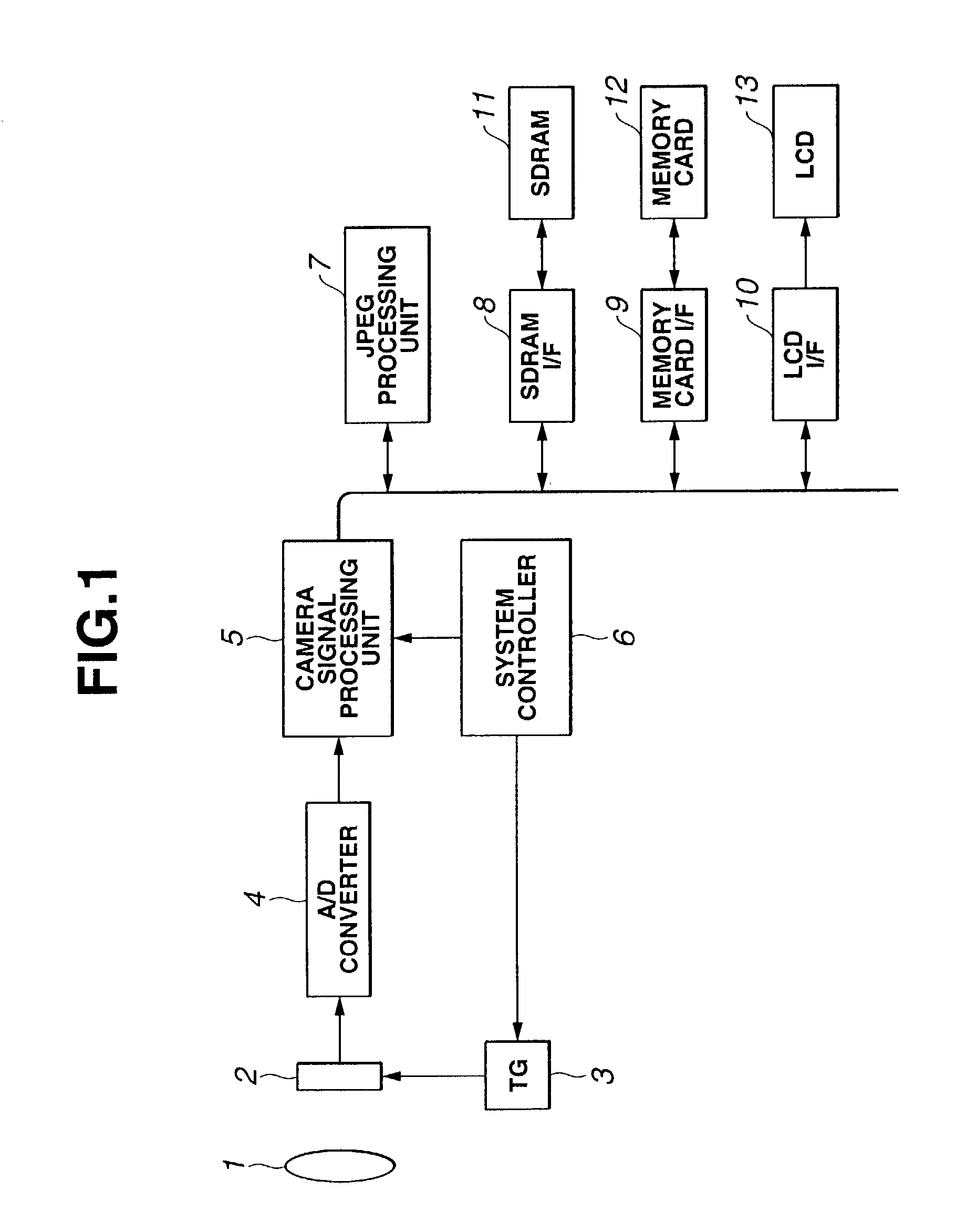
[0041]Embodiments of the present invention will be described with reference to the drawings below. FIG. 1 is a block diagram showing an image pickup apparatus in accordance with the present invention.
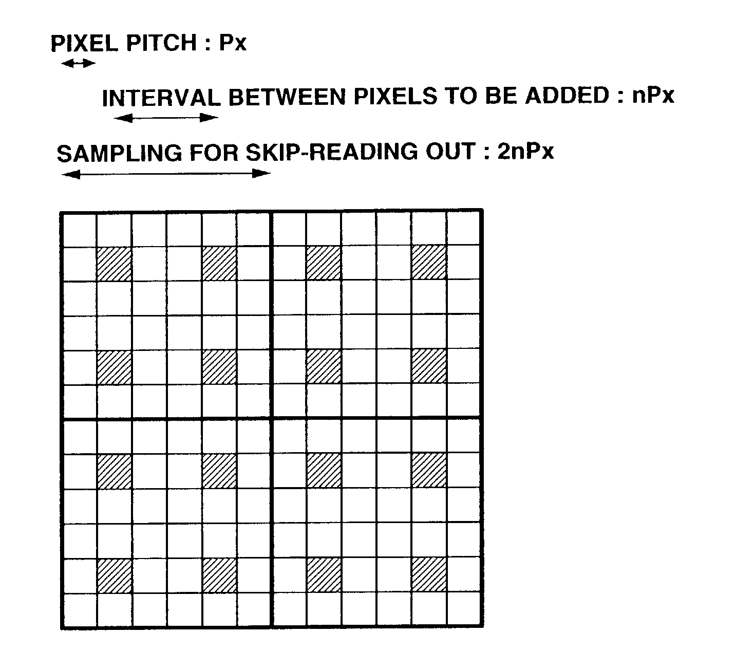
[0042]According to the present embodiment, when pixel skip-reading-out is performed, pixel addition is carried out in order to suppress deterioration in image quality.
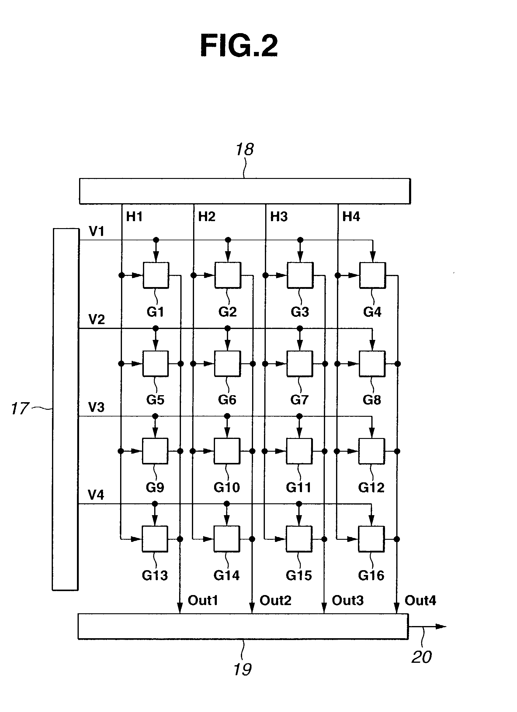
[0043]Referring to FIG. 1, an optical system 1 including an image pickup lens and an optical viewfinder forms an optical image of an object and introduces the optical image to the incidence surface of a solid-state image pickup device 2. The solid-state image pickup device 2 has a plurality of photoelectric converting elements arrayed two-dimensionally, and includes CMOS sensors that can be randomly accessed. Any of the CMOS sensors is accessed by designating x and y addresses, whereby any pixel is read (from a photoelectric converting element). A sensor drive circuit (TG) 3 controls driving of the solid-state image pickup...
second embodiment
[0113]FIG. 15 is a block diagram showing an image pickup apparatus in accordance with the present invention. Referring to FIG. 15, the same reference numerals are assigned to the components identical to those shown in FIG. 1. The present embodiment makes it possible to correct a defect resulting from pixel addition.
[0114]The present embodiment is different from the first embodiment in a point that defect correction circuits 14 and 15, a ROM 16, and a selection circuit (SEL) 17 are additionally included.
[0115]An output of the A / D converter 4 is transferred to the defect correction circuits 14 and 15. The address of a defective pixel location in the solid-state image pickup device is stored in the ROM 16. When all the pixel locations in the solid-state image pickup device 2 are used to define an image pickup area, a signal of a defective pixel contained in the output of the A / D converter 4 is corrected based on the address of a defective pixel location stored in the ROM 16. The result...
PUM
 Abstract
Description
Claims
Application Information


