Cascadable level shifter cell

a level shifter and level shifter technology, applied in the field of electronic devices, can solve the problems of slowness of larger devices, inability to withstand higher voltage levels, and difficult to achieve high-speed switching,

Active Publication Date: 2007-09-11
VLSI TECH LLC
View PDF38 Cites 42 Cited by
  • Summary
  • Abstract
  • Description
  • Claims
  • Application Information

AI Technical Summary

Problems solved by technology

It has proved to be very challenging, however, to provide level shifting and output buffer circuits that interface multiple voltage levels while operating at the desired limits of the I / O speed.
The smaller devices made with the newer technologies have relatively thin gate-oxide layers, which are faster than devices having relatively thick gate-oxide layers, but which are unable to withstand the higher voltage levels.
The larger devices, however, are slower and tend to slow down the I / O interface.
Such drivers suffer from low performance, however, particularly at lower voltage levels of the chip.
Such conventional configuration is susceptible to noise in that any variation in switching voltage at the output of the first caused by noise or the like potentially results in failure to switch the second.

Method used


Image

  • Cascadable level shifter cell
  • Cascadable level shifter cell
  • Cascadable level shifter cell

Examples


Embodiment Construction

[0020]The following description is presented to enable one of ordinary skill in the art to make and use the present invention as provided within the context of a particular application and its requirements. Various modifications to the preferred embodiment will, however, be apparent to one skilled in the art, and the general principles defined herein may be applied to other embodiments. Therefore, the present invention is not intended to be limited to the particular embodiments shown and described herein, but is to be accorded the widest scope consistent with the principles and novel features herein disclosed.

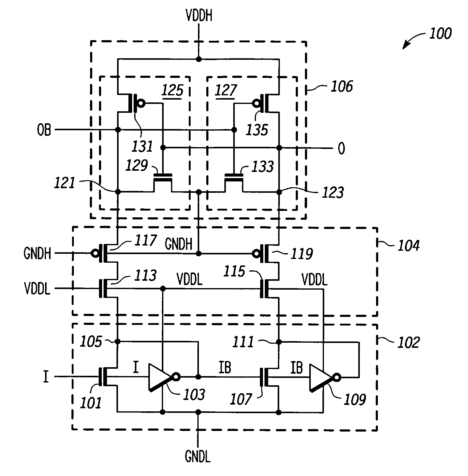
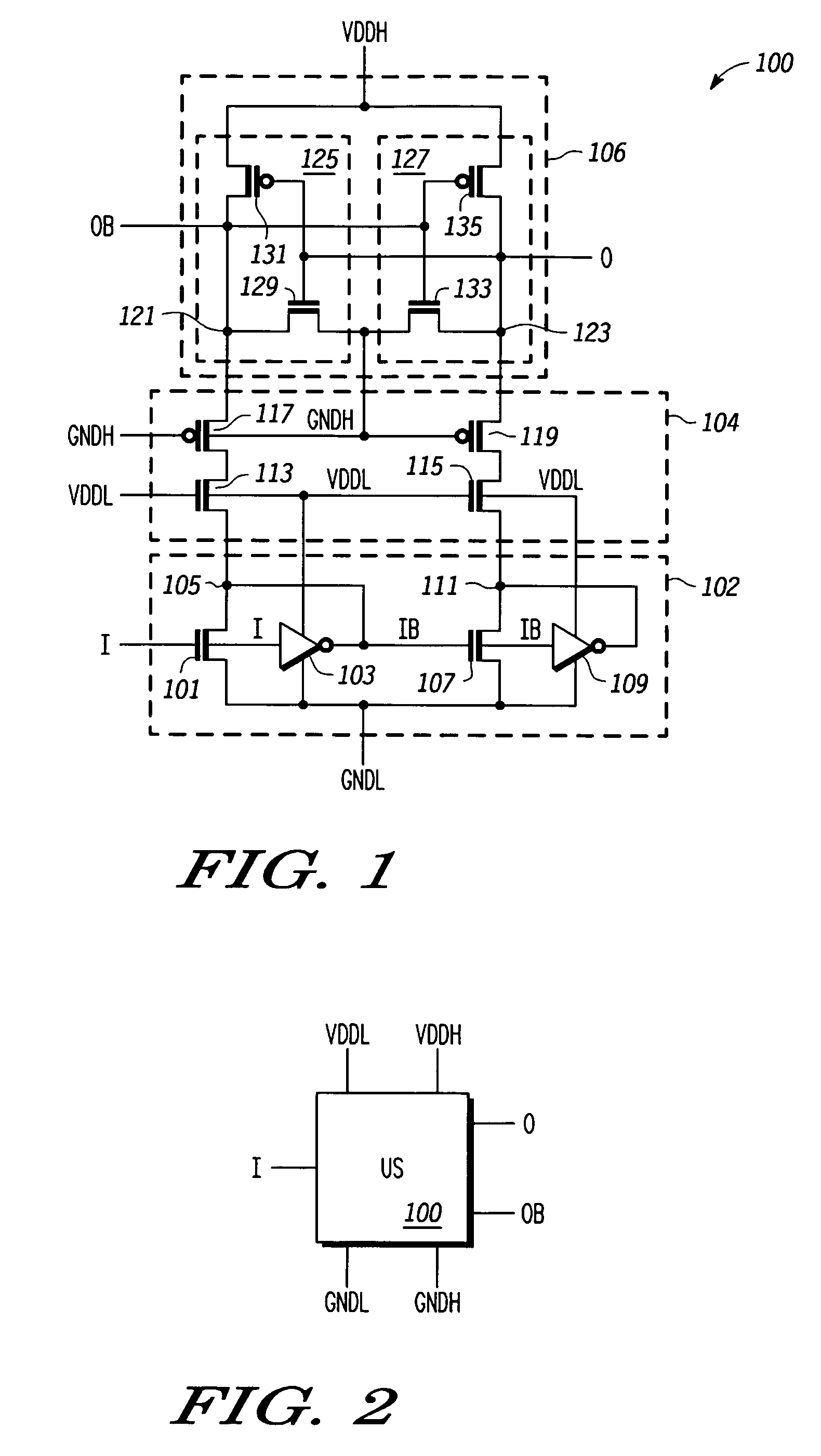
[0021]FIG. 1 is a schematic diagram of an up-shift circuit 100 implemented according to an exemplary embodiment of the present invention. The up-shift circuit 100 includes a lower input circuit 102 coupled to an isolation or protection layer 104, which is further coupled to an upper output circuit 106. An input signal I is provided to the gate of an N-channel transistor 101 and...


PUM


Abstract

A level shifter circuit including first and second circuits and a protection layer. The first circuit receives an input signal and switches first and second nodes to opposite states within a first voltage range between first and second supply voltages. The second circuit switches the third and fourth nodes to opposite states within a second voltage range between third and fourth supply voltages in response to switching of the first and second nodes. The protection layer couples the first and second nodes to third and fourth nodes via respective first and second isolation paths. The isolation paths operate to keep the first and second nodes within the first voltage range and to keep the third and fourth nodes within the second voltage range. Isolation enables the use of thin gate-oxide devices for speed while extending the voltage range beyond the maximum voltage allowable for a single thin gate-oxide device.

Description

BACKGROUND OF THE INVENTION[0001]1. Field of the Invention[0002]The present invention relates in general to electronic devices, and more specifically to a cascadable level shifter cell with improved noise immunity.[0003]2. Description of the Related Art[0004]There exists the need for high-speed, point-to-point interface communications between lower chip level signals, e.g., 1 Volt (V) or less, and external circuits operating at higher voltage levels (e.g, 2.5V, 3.3V, or higher). Many systems include circuitry designed with a variety of technologies operating at multiple voltage levels. It has proved to be very challenging, however, to provide level shifting and output buffer circuits that interface multiple voltage levels while operating at the desired limits of the I / O speed. Process technologies, including CMOS processes, are continually improving resulting in smaller and faster devices, such as, for example, 90-nm CMOS. The smaller devices made with the newer technologies have re...

Claims


Application Information

Patent Timeline
Patent Type & Authority Patents(United States)
IPC IPC(8): H03K19/094
CPCH03K3/356113
Inventor SANCHEZ, HECTORGREAVES, CARLOS A.NISSEN, JIM P.TANG, XINGHAI
Owner VLSI TECH LLC
Why Eureka
Try Eureka