Semiconductor structure having n-channel channel-junction field-effect transistor

a field-effect transistor and semiconductor technology, applied in the field of semiconductor technology, can solve the problems of unsatisfactory gate electrode operation of the igfet, relatively noisy n-channel high-voltage scigfet b>80/b>, etc., and achieve the effect of large noise reduction

Active Publication Date: 2007-02-13
NAT SEMICON CORP
View PDF18 Cites 91 Cited by
  • Summary
  • Abstract
  • Description
  • Claims
  • Application Information

AI Technical Summary

Benefits of technology

[0037]In short, the present invention achieves a very large noise reduction. Fabrication of the complementary-IGFET structure of the invent...

Problems solved by technology

If the drain depletion region punches through to the source depletion region, the operation of the IGFET cannot be controlled with the gat...

Method used


Image

  • Semiconductor structure having n-channel channel-junction field-effect transistor
  • Semiconductor structure having n-channel channel-junction field-effect transistor
  • Semiconductor structure having n-channel channel-junction field-effect transistor

Examples


Embodiment Construction

Reference Notation and Other Conventions

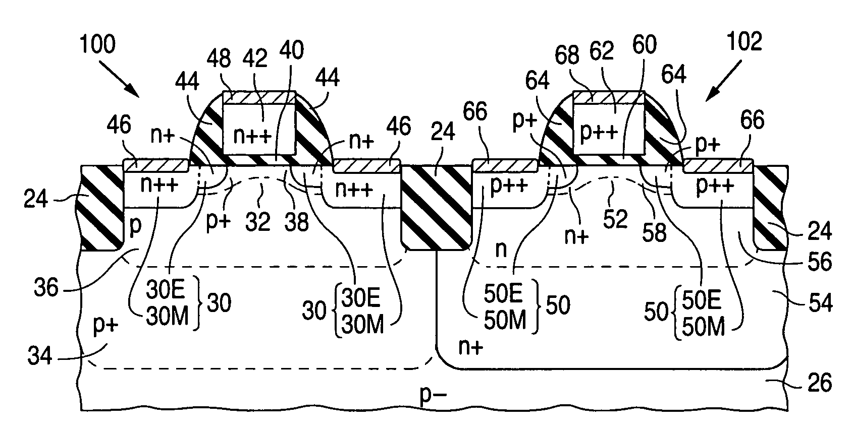
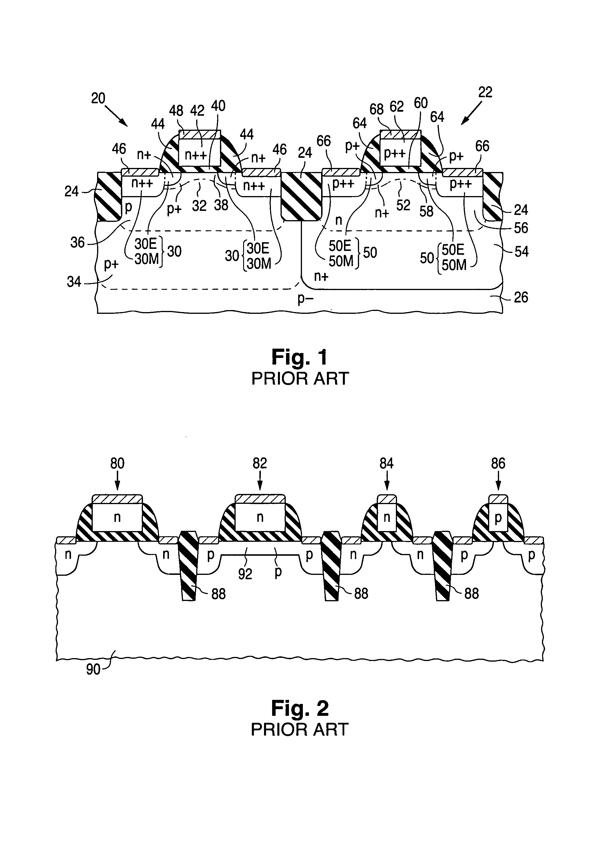
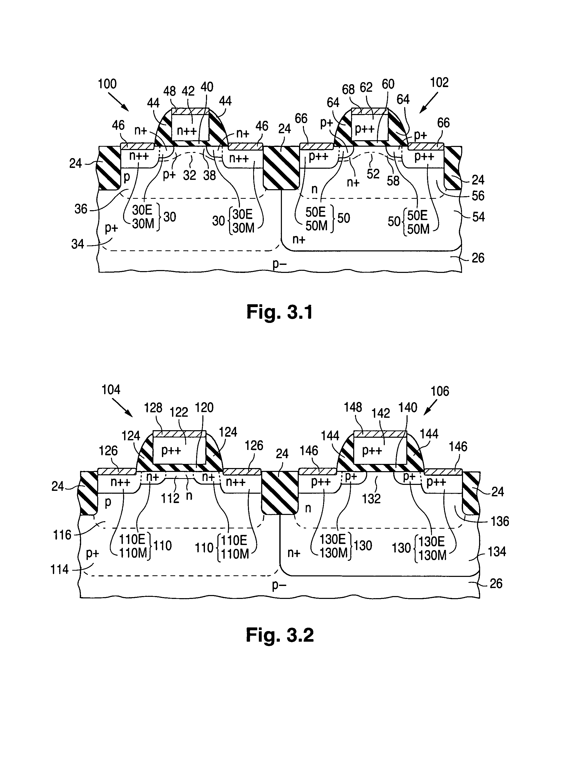
[0050]The reference symbols employed below and in the drawings have the following meanings:[0051]CGD≡gate dielectric capacitance per unit area[0052]DOSENPOLY≡areal dosage of ions of n-type polysilicon gate-electrode dopant[0053]DOSEPPOLY≡areal dosage of ions of p-type polysilicon gate-electrode dopant[0054]EGD≡transversal electric field in gate dielectric layer[0055]EST≡transversal electric field at surface of channel zone at threshold condition[0056]f≡frequency[0057]h≡Planck's constant[0058]L≡channel length along upper semiconductor surface[0059]m0≡free electron mass[0060]m*≡density-of-states effective mass of charge carriers in gate dielectric layer[0061]M≡empirical parameter[0062]MA≡number of azimuthal angles[0063]n≡non-ideality factor[0064]NB≡uniform net dopant concentration in body material[0065]NB0≡background dopant concentration in body material[0066]NC≡uniform net dopant concentration in channel zone[0067]NC0≡net dopant concentration a...


PUM


Abstract

A semiconductor technology combines a normally off n-channel channel-junction insulated-gate field-effect transistor (“IGFET”) (104) and an n-channel surface-channel IGFET (100 or 160) to reduce low-frequency 1/f noise. The channel-junction IGFET is normally of materially greater gate dielectric thickness than the surface-channel IGFET so as to operate across a greater voltage range than the surface-channel IGFET. Alternatively or additionally, the channel-junction IGFET may conduct current through a field-induced surface channel. A p-channel surface-channel IGFET (102 or 162), which is typically of approximately the same gate-dielectric thickness as the n-channel surface-channel IGFET, is preferably combined with the two n-channel IGFETs to produce a complementary-IGFET structure. A further p-channel IGFET (106, 180, 184, or 192), which is typically of approximately the same gate dielectric thickness as the n-channel channel-junction IGFET, is also preferably included. The further p-channel IGFET can be a surface-channel or channel-junction device.

Description

FIELD OF USE[0001]This invention relates to semiconductor technology and, in particular, to field-effect transistors of the insulated-gate type.BACKGROUND ART[0002]An insulated-gate field-effect transistor (“IGFET”) is a semiconductor device in which a gate dielectric layer electrically insulates a channel zone of a semiconductor body from an overlying gate electrode. The channel zone extends between a source and a drain that adjoin a body region of the semiconductor body. The body region, often referred to as the substrate region or substrate, is of opposite conductivity type to the source and drain. Charge carriers, i.e., electrons for an n-channel IGFET and holes for a p-channel IGFET, move from the source through the channel zone to the drain when appropriate voltages are applied to the gate electrode, source, drain, and body region. By suitably controlling these voltages, the IGFET switches between on and off conditions.[0003]The terms “normally off” and “normally on” are commo...

Claims


Application Information

Patent Timeline
IPC IPC(8): H01L29/76
CPCH01L21/823807H01L27/0883H01L29/7833H01L29/1041H01L29/105H01L27/0928H01L21/26586H01L29/665
Inventor BULUCEA, CONSTANTINLINDORFER, PHILIPP
Owner NAT SEMICON CORP
Why Eureka
Try Eureka