Optical waveguide device, manufacturing method for optical waveguide device and intermediate of optical waveguide device

a technology of optical waveguide and manufacturing method, which is applied in the direction of optical waveguide light guide, instruments, optics, etc., can solve the problems of wrinkles and voids, inner stress in resin dispersions, and decrease of voids, so as to reduce the characteristic deterioration and appearance failure of waveguide equipment.

Inactive Publication Date: 2007-09-11
ORMON CORP
View PDF9 Cites 0 Cited by
  • Summary
  • Abstract
  • Description
  • Claims
  • Application Information

AI Technical Summary

Benefits of technology

[0011]Embodiments of the present invention prevent the wrinkle by cure shrinkage of the cladding layer from occurring, and decrease the characteristic deterioration and the appearance failure in waveguide equipment.
[0014]For waveguide equipment in accordance with one or more embodiments of the present invention, the thickness of the lower cladding layer becomes precise to be supported the upper cladding layer with the spacer. In addition, each of the difference of the height between the top surface of the spacer and the intermediate surface, the difference of the height between the intermediate surfaces, and the difference of the height between the intermediate surface and the inner bottom surface of the recess of the second substrate becomes thinner than the total thickness of the lower cladding layer. Thus, when the resin for the lower cladding layer is cured to shrinkage, the inner stress in the resin disperses and the occurrence of the wrinkle and the void decreases. The appearance failure and the characteristic deterioration in the waveguide equipment are prevented.

Problems solved by technology

Thus, when the resin for the lower cladding layer is cured to shrinkage, the inner stress in the resin disperses and the occurrence of the wrinkle and the void decreases.

Method used


Image

  • Optical waveguide device, manufacturing method for optical waveguide device and intermediate of optical waveguide device
  • Optical waveguide device, manufacturing method for optical waveguide device and intermediate of optical waveguide device
  • Optical waveguide device, manufacturing method for optical waveguide device and intermediate of optical waveguide device

Examples


Embodiment Construction

[0043]Specific embodiments of the present invention are explained in detail below with reference to the figures. These embodiments are merely examples and the present invention is not limited to the specific embodiments explained below.

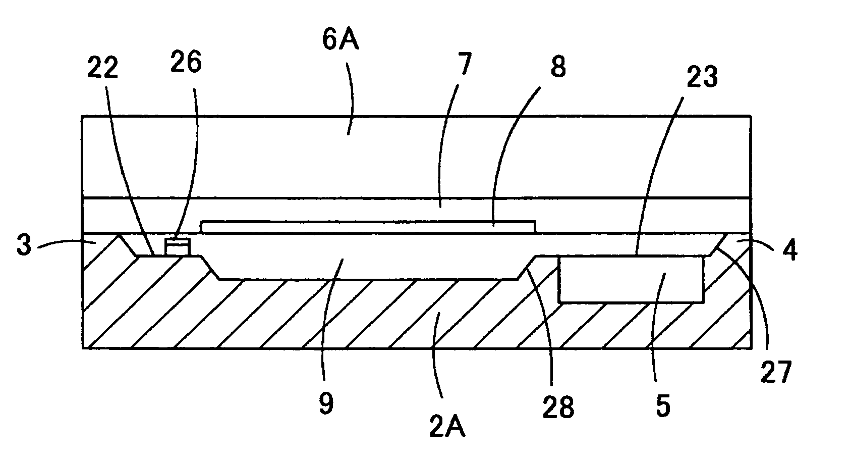
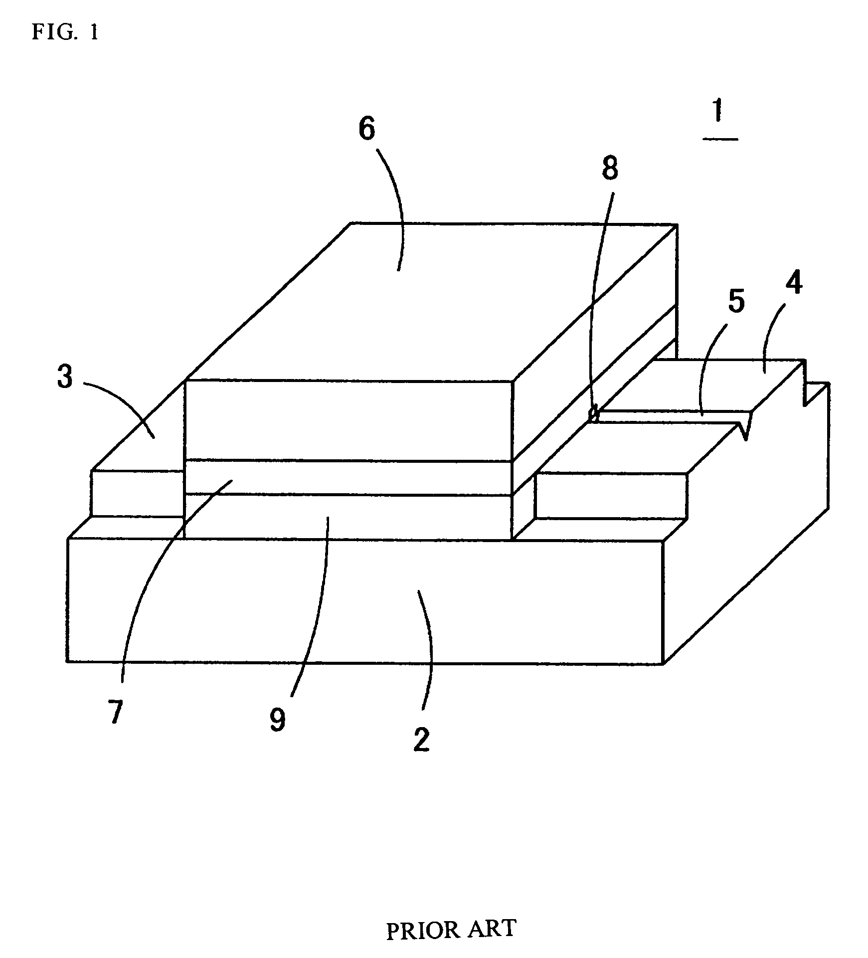
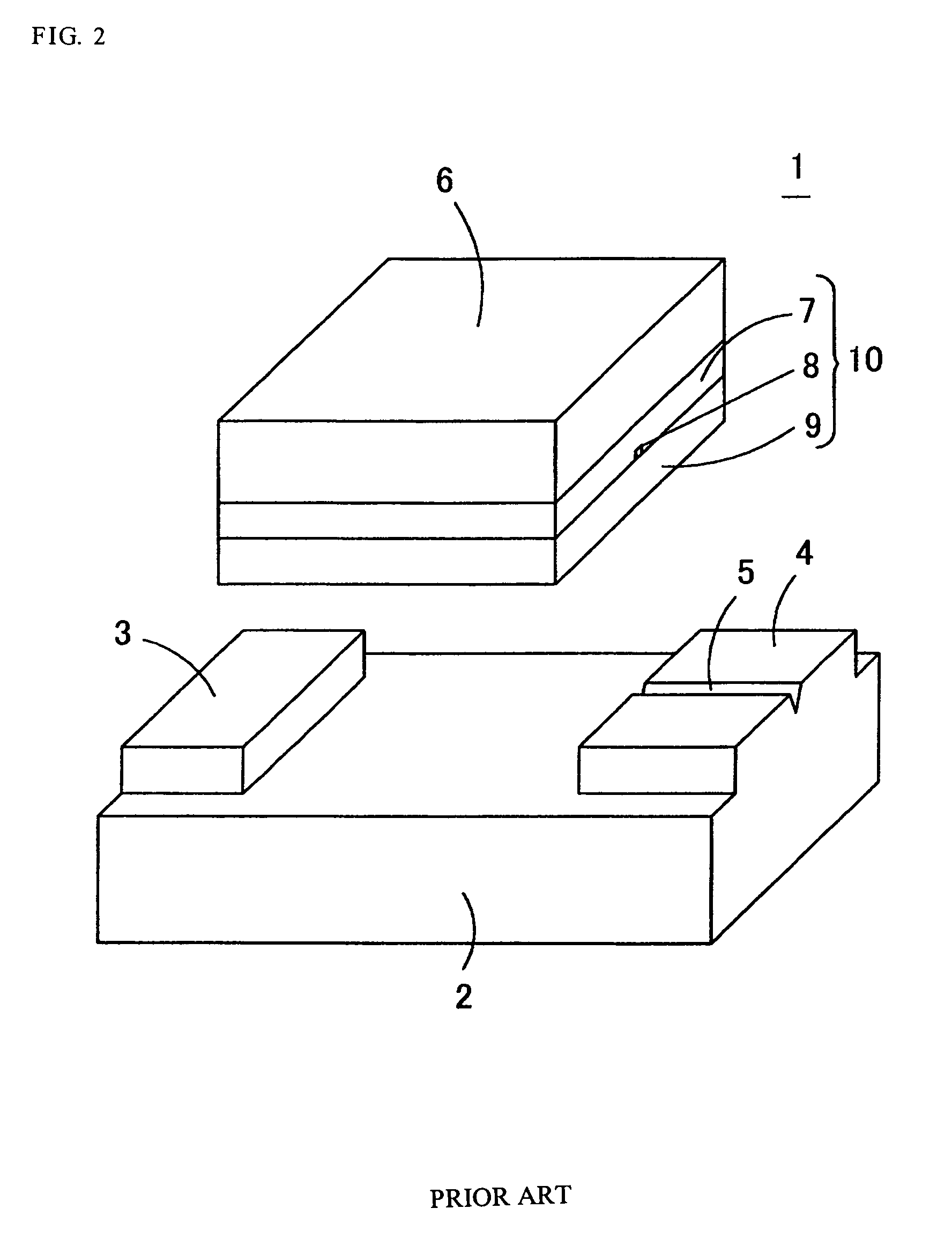
[0044]FIG. 8 is a perspective view showing waveguide equipment 21 in accordance with one embodiment of the present invention. FIG. 9 is an exploded perspective view showing the waveguide equipment 21 which is one step before the finished product. FIG. 10 is a plan view showing a gathering of the waveguide equipment 21 in a manufacturing process. FIG. 11 is a sectional view of FIG. 10 cut by X3-X3 line. The waveguide equipment 21 of this embodiment has the same structure and is produced by the same process as the waveguide equipment 1 shown in FIG. 1 to FIG. 4. The parts which are the same are not explained in detail below . The description of such parts is omitted and such parts have the same numbers in the drawings as numbers in the waveguide equipme...


PUM


Abstract

The spacers 3 and 4 and the recess is formed on the supporting substrate 2 to support the upper cladding layer 7. The intermediate surface 22 and 23 lower than the top surface of the spacers 3 and 4 and higher than the inner bottom surface of the recess is formed on the supporting substrate 2. Each of the height between the top surface of the spacers 3 and 4 and the intermediate surfaces 22 and 23, and the height between the intermediate surfaces 22 and 23 and the inner bottom surface of the recess of the second substrate 2 becomes thin compared with the total thickness of the lower cladding layer. Thus, when the resin for the lower cladding layer 9 is cured to shrinkage, the inner stress in the resin is dispersed and the occurrence of the wrinkle 12 and the void decreases.

Description

BACKGROUND OF THE INVENTION[0001]1. Field of the Invention[0002]The invention relates generally to waveguide equipment, production methods thereof, and intermediates thereof.[0003]2. Background Art[0004]In a connected portion and an end portion of an optical fiber cable for optical communications, waveguide equipment is used to connect the end of one optical fiber cable to, for example, another optical fiber cable, a light projection device, a photo detector, etc. Such waveguide equipment has been made of a quartz material of low loss in an infrared wavelength region. Recently, waveguide equipment with a polymer waveguide has been made of polymer material with low cost. For example, the waveguide equipment comprises the polymer waveguide on a silicon substrate.[0005]Inventors of the present invention produced the waveguide equipment shown in FIG. 1 and FIG. 2. FIG. 1 is a perspective view of the waveguide equipment 1, and FIG. 2 is an exploded perspective view thereof. The waveguide...

Claims


Application Information

Patent Timeline
Patent Type & Authority Patents(United States)
IPC IPC(8): G02B6/10G02B6/12G02B6/122G02B6/13G02B6/30G02B6/36G02B6/42
CPCG02B6/1221G02B6/30G02B6/3636G02B6/42G02B6/3652G02B6/3692G02B6/423
Inventor KOMURA, YOSHIYUKIHAYAMIZU, KAZUYUKIHIGUCHI, MASAYOSHITANIGUCHI, HISASHITERAKAWA, YUKARIHOSOKAWA, HAYAMI
Owner ORMON CORP
Why Eureka
Try Eureka