Solution applying apparatus and method

a technology of solution and applying apparatus, which is applied in the direction of electrical equipment, basic electric elements, semiconductor/solid-state device manufacturing, etc., can solve the problems of unsatisfactory solution circulation, island-shaped etching irregularities over the entire surface of the substrate, and insufficient wet etching solution, etc., to achieve good solution circulation and good solution circulation

Inactive Publication Date: 2007-09-18
SEMICON ENERGY LAB CO LTD
View PDF46 Cites 7 Cited by
  • Summary
  • Abstract
  • Description
  • Claims
  • Application Information

AI Technical Summary

Benefits of technology

[0016]The object of the present invention is to provide a solution applying apparatus and method for uniformly applying a solution using a desired solution applying (dropping or flowing) method, in a solution applying method such as spin etching in which an etching solution moves on an etching surface at a high speed and has good solution circulation.
[0045]In general, the contact angle of an etching solution with respect to the resist is reduced by irradiating ultraviolet light to the hardened resist for a desired period, or bringing it into contact with ozone water (water in which ozone (O3) has dissolved at 0.1 to 20 ppm), so that and a wetting degree of the etching solution is greatly increased.
[0046]The present invention makes use of this phenomenon, and before applying the solution, ultraviolet light is irradiated to the patterned and hardened resist which is formed on the substrate, or the resist is brought in contact with ozone water. It is thus possible to perform uniform etching without irregularities within a single substrate surface, even using an etching solution with a large contact angle, in an etching method in which the moving speed of the etching solution over the surface to be etched is fast, for example, spin etching.
[0047]Further, even with fine patterns in which the pattern width is of the order of several μm or less, since an etching solution penetrates adequately between the resists forming the pattern, uniform etching is possible.
[0048]It is even possible to prevent the occurrence of etching irregularities when the substrate is large.
[0049]As an effect which a solution is applied (added) sufficiently by ultraviolet light irradiation or ozone water processing, the following can be considered. That is, by ultraviolet light irradiation and ozone water contact to the hardened resist, an organic substance (or an organic contamination) on the surface of the resist is decomposed and removed and simultaneously the surface of the resist is activated, so that a surface energy of the resist decreases and a contact angle to a solution becomes small. Ultraviolet light irradiation is more effectively performed in an oxygen atmosphere since reactivity with an organic substance is increased.

Problems solved by technology

When spin etching is performed using an etching solution which has a large contact angle with respect to the resist, for example, hydrofluoric acid based etching solutions in a wet etching process, the etching solution does not adequately wet the surface to be etched, so that the etching solution forms balls and flows off.
As a result, island-shaped etching irregularities form over the entire surface of the substrate.
That is, since an etching solution does not penetrate uniformly into the fine portion, solution circulation is liable to be unsatisfactory.
In other words, if the area of the substrate increases, contact between the etching solution and the surface of the substrate is liable to be nonuniform.
Also, irregularities also occur in the spray method (2).
In a liquid crystal display device, since several hundred thousand thin film transistors (TFTs) are formed on a single substrate such as quartz or glass in the same process, defect of one TFT causes defect of a substrate.
Therefore, irregularity of the above etching causes the decrease of yield.
However, if the solution containing a metal element is uniformly added, since an amorphous silicon film is not crystallized sufficiently, characteristics of elements on the same substrate are different from each other.
However, it takes trouble.

Method used


Image

  • Solution applying apparatus and method
  • Solution applying apparatus and method
  • Solution applying apparatus and method

Examples


embodiment 1

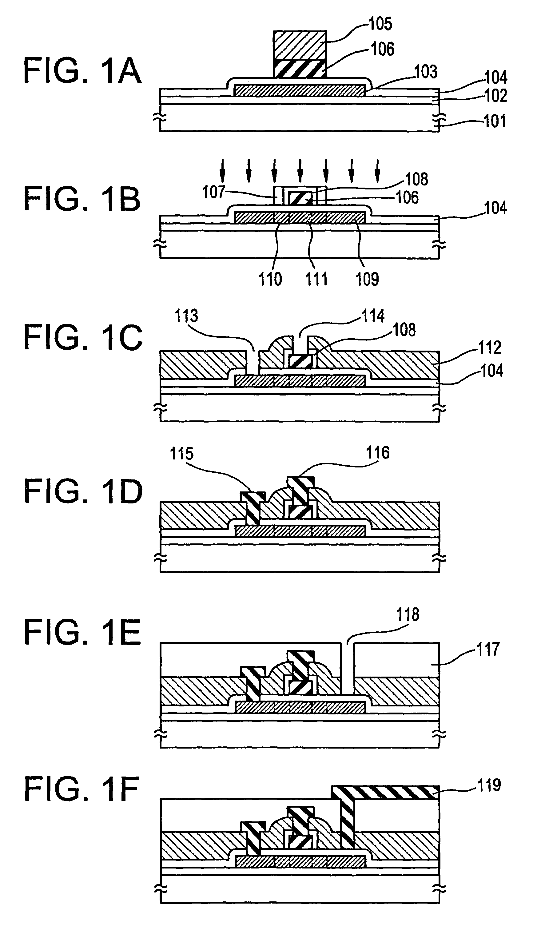
[0065]In the embodiment, a process in which ultraviolet light is irradiated is performed before the etching process in the manufacture of a P channel-type pixel thin film transistor (TFT) used in an active matrix type liquid crystal electro-optical device. FIGS. 1A to 1F show the forming processes of the P-channel type pixel TFT in the embodiment.

[0066]In FIG. 1A, a silicon oxide film is formed to a thickness of 3000 Å by sputtering as a base film 102 on a glass substrate 101 (Corning #7059, 100 mm×100 mm). An amorphous silicon film is then formed to a thickness of 500 Å by plasma CVD, and then crystallization is performed by the thermal annealing in a nitrogen atmosphere for 12 hours at 600° C. Further, laser annealing is performed to improve crystallization. The energy density of the laser is suitably 250 to 350 mJ / cm2, in the embodiment, 300 mJ / cm2.

[0067]An island-like silicon film 103 is formed by patterning the crystallized silicon film. The silicon film 103 forms the active la...

embodiment 2

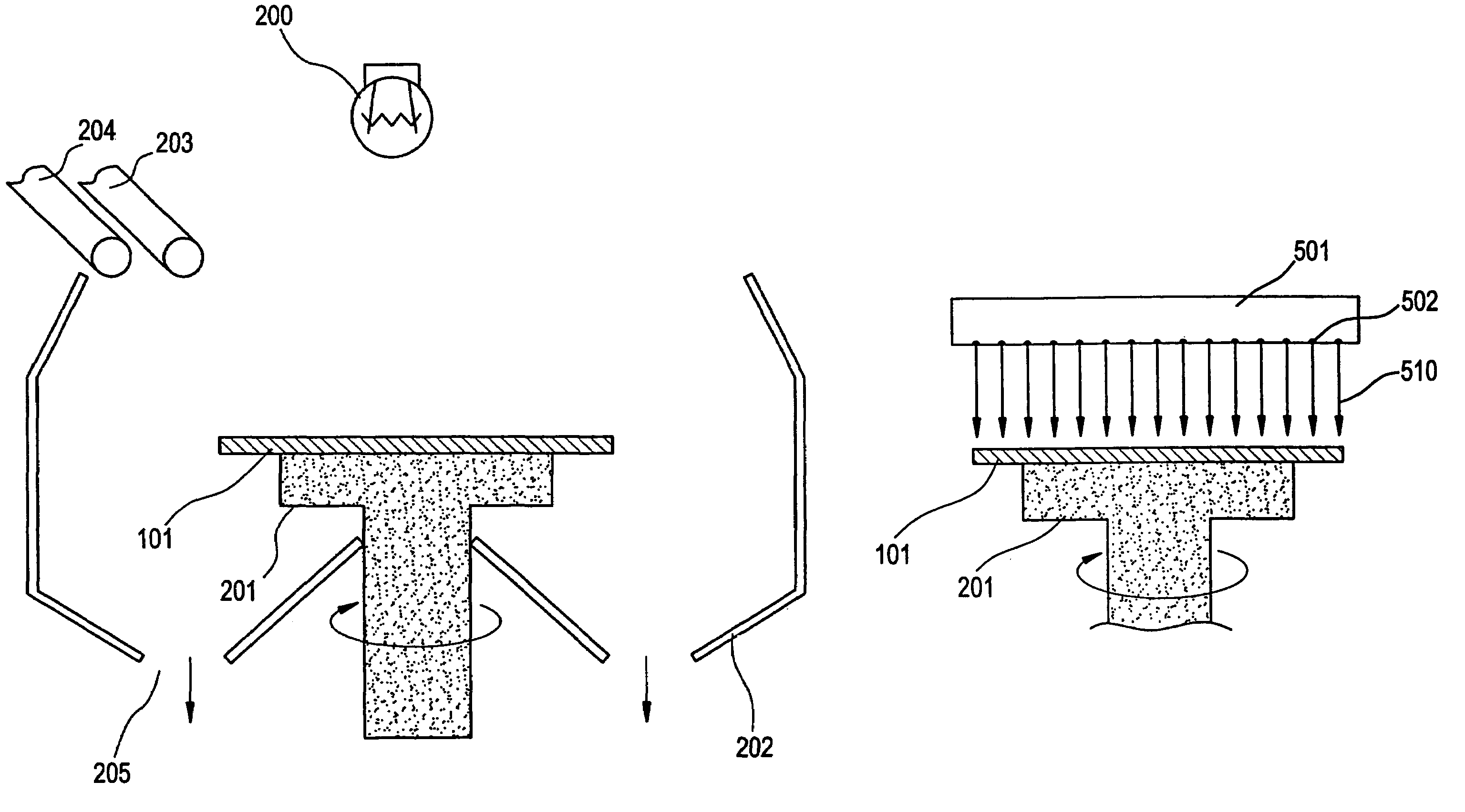
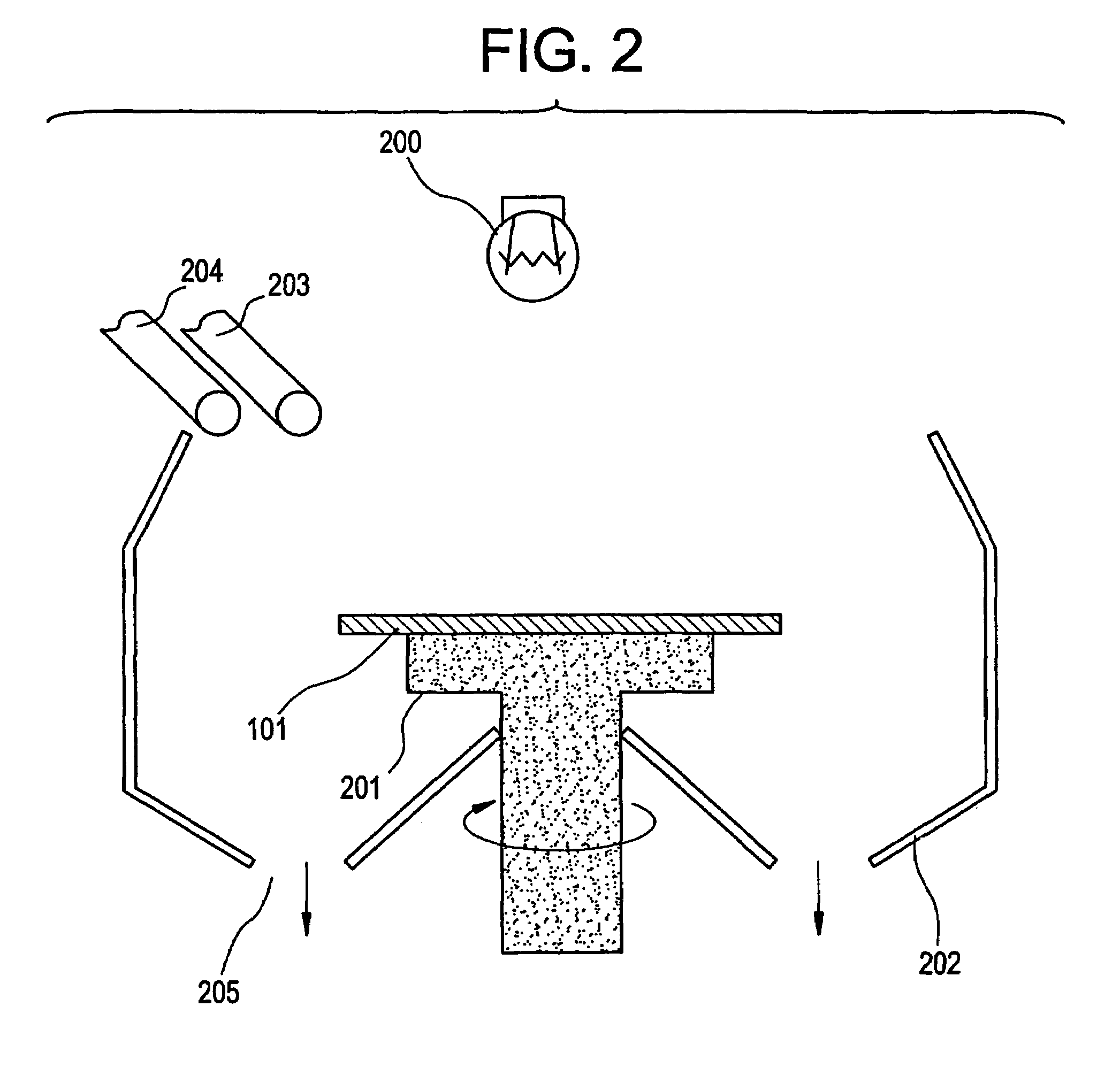
[0096]The embodiment is an example of a spin etching system in which a spin etching apparatus and other apparatuses are provided integrally, as shown in FIG. 3. A robot arm 302 for moving the substrate 101 is provided at the center on a main body 301. A cassette 303 which houses a plurality of substrates 101, a substrate positioning (alignment) unit 304 and a spin etching apparatus 305 are provided such that they surround the robot arm 302. An ultraviolet light irradiating unit 304a such as a high pressure mercury lamp which irradiates ultraviolet light from the top is provided in the positioning unit 304, and therefore ultraviolet light can be irradiated at the same time as positioning is effected, and therefore the process is simplified.

[0097]In FIG. 3, a first nozzle which causes an etching solution to flow, and a second nozzle which causes pure water to flow for washing are provided in the spin etching apparatus 305, and thus washing, etching and drying (spin drying) can be perf...

embodiment 3

[0099]The embodiment is an example of processes in which ozone water is brought into contact with the resist prior to the etching process, and in which a P channel-type pixel TFT, as used in an active matrix type liquid crystal electro-optical device, is formed. The manufacturing process for the P-channel type pixel TFT of the embodiment is shown in FIGS. 1A to 1F.

[0100]In FIG. 1A, a silicon oxide film is formed to a thickness of 3000 Å by sputtering as a base film 102 on a glass substrate 101 (Corning #7059, 100 mm×100 mm). An amorphous silicon film is then formed to a thickness of 500 Å by plasma CVD, and then which crystallization is performed by the thermal annealing in a nitrogen atmosphere for 12 hours at 600° C. Further, laser annealing is performed to improve crystallization. The energy density of the laser is suitably 250 to 350 mJ / cm2, in the embodiment 300 mJ / cm2.

[0101]An island-like silicon film 103 is formed by patterning the crystalline silicon film formed in this way....


PUM


Abstract

In etching using an etching solution, irradiating ultraviolet light is irradiated into a resist patterned on an etching substrate or a film formed on the etching substrate and then an etching solution is applied to the etching substrate while rotating the etching substrate. Also, ozone water is applied in contact with the resist and then an etching solution is applied to the etching substrate while rotating the etching substrate. In crystallization using a metal element such as nickel for promoting crystallization of silicon, irradiating ultraviolet light is irradiated into a resist patterned on an substrate or a film formed on the substrate and then a nickel solution is applied to the substrate while rotating the substrate. Also, ozone water is applied in contact with the resist and then the nickel solution is applied to the substrate while rotating the substrate.

Description

[0001]This application is a Div of Ser. No. 09 / 572,730 May 17, 2000 ABN which is a Div of Ser. No. 08 / 533,204 Sep. 25, 1995 and issued as U.S. Pat. No. 6,127,279.BACKGROUND OF THE INVENTION[0002]1. Field of the Invention[0003]The present invention relates to a solution applying apparatus and a solution applying method used for a technique for applying a solution, such as wet etching, in a forming technique for a semiconductor device.[0004]2. Description of the Related Art[0005]Processes for applying a solution to a substrate are often performed when manufacturing semiconductor devices such as thin film transistors (TFTs) in which thin films of semiconductor, insulator and metal or the like are laminated and formed on a semiconductor substrate or glass substrate, such as semiconductor integrated circuits, active matrix type liquid crystal electro-optical devices and the like.[0006]Commonly used solution applying methods has (1) a method for immersing (dipping) a substrate into a bath...

Claims


Application Information

Patent Timeline
Patent Type & Authority Patents(United States)
IPC IPC(8): H01L21/461H01L21/00H01L21/02H01L21/311H01L21/3213
CPCH01L21/02071H01L21/31111H01L21/32134H01L21/6708
Inventor KONUMA, TOSHIMITSU
Owner SEMICON ENERGY LAB CO LTD
Why Eureka
Try Eureka