Defective pixel detection and correction apparatus using target pixel and adjacent pixel data

a technology of defective pixels and correction apparatus, applied in the direction of color signal processing circuits, television system scanning details, television systems, etc., can solve the problem of inability to detect defective pixels correctly

Inactive Publication Date: 2007-10-09
PANASONIC CORP
View PDF6 Cites 14 Cited by
  • Summary
  • Abstract
  • Description
  • Claims
  • Application Information

AI Technical Summary

Benefits of technology

[0007]It is, therefore, one objective of the present invention to provide a solid-state imaging apparatus having a defective pixel correction function that can correct the output signal for a defective pixel without spreading the effect produced by the defective pixel to a peripheral pixel.

Problems solved by technology

Therefore, the effect produced by the defective pixel spreads to the pixel data for the peripheral pixels, and it is impossible for the defective pixel to be detected correctly and the pixel data therefor to be corrected.

Method used


Image

  • Defective pixel detection and correction apparatus using target pixel and adjacent pixel data
  • Defective pixel detection and correction apparatus using target pixel and adjacent pixel data
  • Defective pixel detection and correction apparatus using target pixel and adjacent pixel data

Examples


Embodiment Construction

[0028]One embodiment of the present invention will now be described while referring to the drawings.

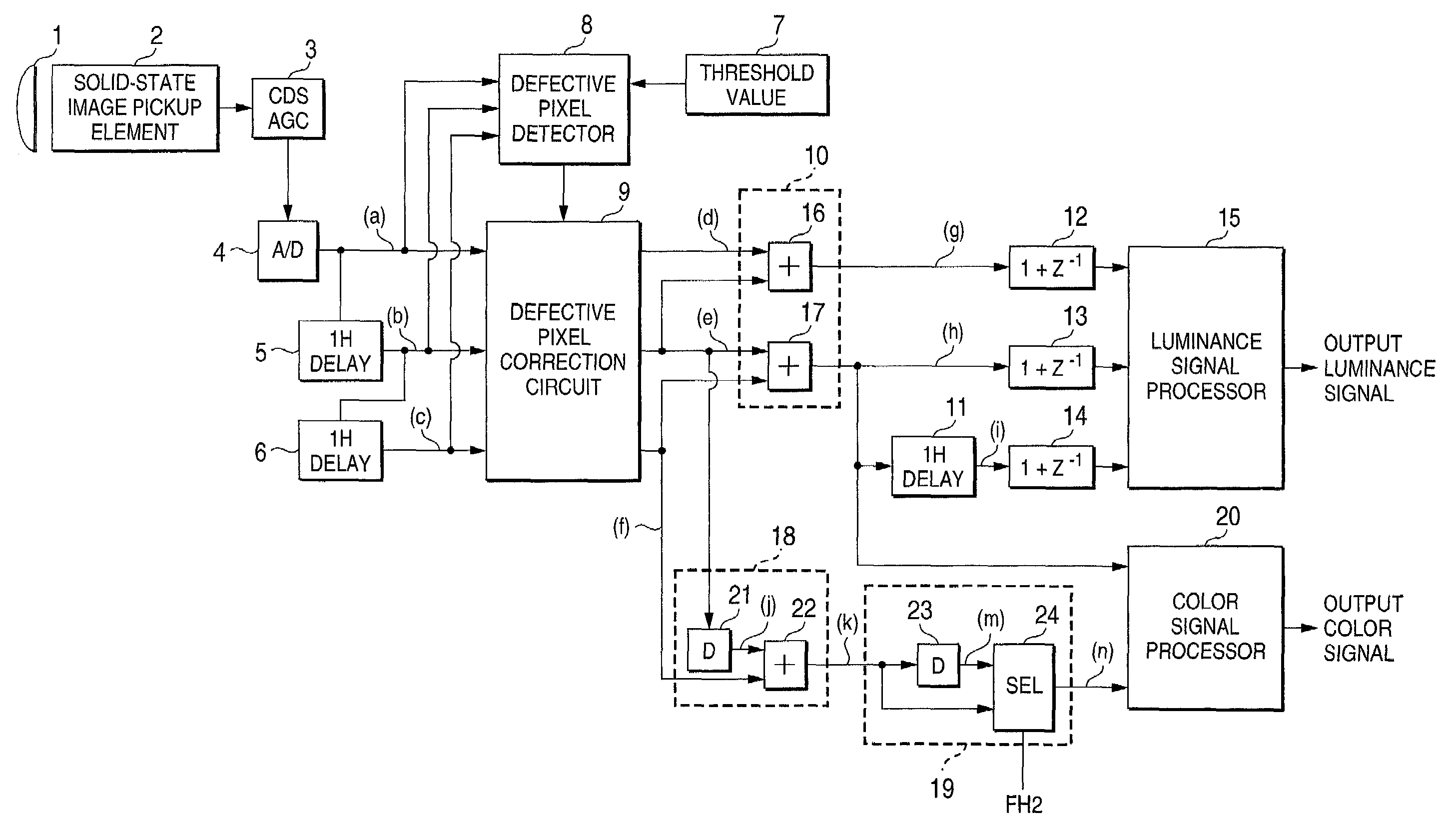
[0029]FIG. 1 is a diagram showing the configuration of a solid-state imaging apparatus according to the embodiment of the present invention. This solid-state imaging apparatus includes: a lens 1; a frame-reading solid-state image pickup element (hereinafter referred to simply as a “solid-state image pickup element”) that is located at the point of focus of the lens 1; a pre-processor 3 for pre-processing the output signal of the solid-state image pickup element 2 (this preprocessor includes a CDS (Correlated Double Sampling) circuit for sampling a signal and holding the sampled signal and an AGC (Automatic Gain Control) circuit for providing automatic gain control); and an A / D converter 4 for converting into a digital signal an analog signal output by the pre-processor 3.

[0030]The solid-state imaging apparatus further includes; a 1 H delay circuit 5 for delaying the A / D converter 4 ou...


PUM


Abstract

A solid-state imaging apparatus includes: a defective pixel detector (8) for extracting, from a signal output by a frame-reading solid-state image pickup element (2), pixel data for a target pixel for which a determination is to be made and pixel data for peripheral pixels thereof, and for employing pixel data for a pixel, selected from among the peripheral pixels, in the same filter as the target pixel, to determine whether the target pixel is a defective pixel; and a defective pixel correction circuit (9) for employing the pixel data for the peripheral pixels to correct pixel data for the defective pixel. With this configuration, the output signal of the defective pixel can be corrected without spreading the effect produced by the defective pixel to the peripheral pixels, and a natural image can be displayed.

Description

BACKGROUND OF THE INVENTION [0001]The present invention relates to a solid-state imaging apparatus having a solid-state image pickup element used for a video camera, and relates in particular to a solid-state imaging apparatus having a correction device for correcting a signal that is output by a solid-state image pickup element for a defective pixel.[0002]FIG. 10 is a diagram showing the configuration of a conventional solid-state imaging apparatus having a defective pixel correction function, which is disclosed in Japanese Patent Publication No. Hei. 5-41868. In the conventional solid-state imaging apparatus, image data is detected through a lens 101 by a frame-reading image pickup element. The obtained image signal is pre-processed by a pre-processor 103, and the resultant signal is converted into a digital image signal by an A / D converter 104.[0003]This digital image signal is delayed one horizontal scanning period by a 1 H delay circuit 105, and is further delayed one horizonta...

Claims


Application Information

Patent Timeline
Patent Type & Authority Patents(United States)
IPC IPC(8): H04N9/64H04N3/14H04N5/335H04N9/04H04N9/083H04N5/367H04N9/07
CPCH04N9/045H04N5/3675H04N25/683H04N23/84H04N25/136
Inventor TOYODA, KEIJISUGIOKA, YUICHIROKARIYA, MASAKI
Owner PANASONIC CORP
Why Eureka
Try Eureka