Phase change random access memory device having variable drive voltage circuit

a random access and memory device technology, applied in the field of phase change memory devices, can solve problems such as complicated circuit schemes and manufacturing processes

Active Publication Date: 2007-10-16
SAMSUNG ELECTRONICS CO LTD
View PDF16 Cites 44 Cited by
  • Summary
  • Abstract
  • Description
  • Claims
  • Application Information

AI Technical Summary

Problems solved by technology

These differing voltage requirements can result in complicated circuit schemes and manufacturing processes.

Method used


Image

  • Phase change random access memory device having variable drive voltage circuit
  • Phase change random access memory device having variable drive voltage circuit
  • Phase change random access memory device having variable drive voltage circuit

Examples


Embodiment Construction

[0042]The present invention will now be described more fully with reference to the accompanying drawings, in which exemplary embodiments of the invention are shown. The invention may, however, be embodied in many different forms and should not be construed as being limited to the embodiments set forth herein; rather, these embodiments are provided so that this disclosure will be thorough and complete, and will fully convey the concept of the invention to those skilled in the art. Like reference numerals in the drawings denote like elements, and thus their descriptions will not be repeated.

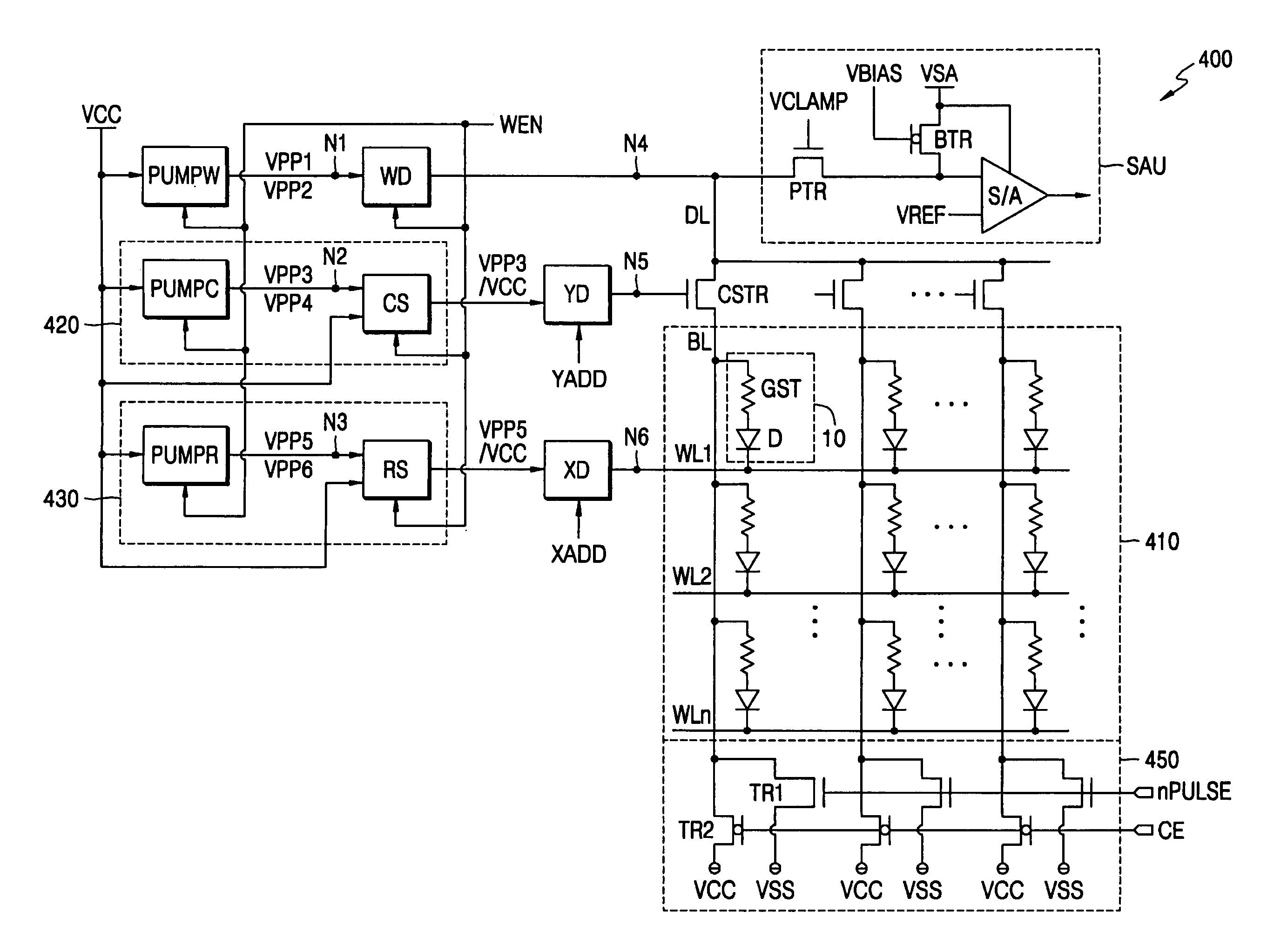
[0043]Referring to FIG. 4, the phase change memory device 400 includes a memory array 410, a memory array controller 450, a plurality of column select transistors CSTR, a sense amplifier SAU, a column decoder YD, a row decoder XD, a write driver WD, a column drive selector CS, a row drive selector RS, and boosting circuits PUMPW, PUMPC and PUMPR. The column boosting circuit PUMPC and the column sel...


PUM


Abstract

A phase change memory device includes a memory array including a plurality of phase change memory cells, each phase change memory cell including a phase change material and a diode, a plurality of column selection transistors connecting bit lines connected to the phase change memory cells to corresponding data lines, and a control node connecting the data lines to a sense amplifier unit. In a write operation mode, control voltages obtained by boosting a first voltage are respectively applied to the control node and gates of the column selection transistors, and a ground voltage is applied to a word line of a selected one of the phase change memory cells. In a standby mode, word lines and bit lines connected to the phase change memory cells of the memory array are maintained at the same voltage. According to the phase change memory device and a driving method thereof, a sufficient write voltage is supplied to a write driver, a column decoder and a row decoder in the write operation mode, and a voltage lower is applied to the write driver, the column decoder and the row decoder in the read operation mode and the standby mode, thereby reducing current consumption and enhancing operational reliability.

Description

BACKGROUND OF THE INVENTION[0001]1. Field of the Invention[0002]The present invention generally relates to semiconductor memory devices, and more particularly, the present invention relates to a phase change memory devices.[0003]A claim of priority is made to Korean Patent Application No. 10-2005-0083581, filed on Sep. 8, 2005, in the Korean Intellectual Property Office, the disclosure of which is incorporated herein in its entirety by reference.[0004]2. Description of the Related Art[0005]A phase-change random access memory (PRAM), also known as an Ovonic Unified Memory (OUM), includes a phase-change material such as a chalcogenide alloy which is responsive to energy (e.g., thermal energy) so as to be stably transformed between crystalline and amorphous states. Such a PRAM is disclosed, for example, in U.S. Pat. Nos. 6,487,113 and 6,480,438.[0006]The phase-change material of the PRAM exhibits a relatively low resistance in its crystalline state, and a relatively high resistance in ...

Claims


Application Information

Patent Timeline
Patent Type & Authority Patents(United States)
IPC IPC(8): G11C11/00G11C5/14
CPCG11C13/0004G11C13/0038G11C13/0069G11C13/004G11C2213/72G11C2013/009G11C13/02
Inventor CHO, WOO-YEONGKIM, DU-EUNGLEE, KWANG-JINKWAK, CHOONG-KEUN
Owner SAMSUNG ELECTRONICS CO LTD
Why Eureka
Try Eureka