Method for conforming a micro-electronic array to arbitrary shapes

a micro-electronic array and shape technology, applied in the field of micro-electronic array formation, can solve the problems of low electrical resistance between metals, insufficient steradian, and limited current semiconductor technology in its ability to form curved structures containing high densities of active components

Active Publication Date: 2007-11-06
HRL LAB
View PDF2 Cites 25 Cited by
  • Summary
  • Abstract
  • Description
  • Claims
  • Application Information

AI Technical Summary

Problems solved by technology

However, current semiconductor technology is limited in its ability to form curved structures containing high densities of active components.
While a curvature occurred, one steradian is insufficient if attempting to conform the semiconductor device to a sphere.
A problem associated with stretching flexible film is that electrical resistance degradation occurs between the metals used to interconnect the discrete devices.
Metal in tension is also more likely to fail from cracking.
The approaches described above are limited in the variety of shapes that can be conformed to and their general applicability to a wide set of device or sensor technologies.
Additionally, the prior art relies on deforming the active device itself, which requires thinning the initially rigid material for curvature to be accomplished.
Bending or deforming the active components can introduce serious performance degradation by increasing the resistance between the metal interconnects.

Method used


Image

  • Method for conforming a micro-electronic array to arbitrary shapes
  • Method for conforming a micro-electronic array to arbitrary shapes
  • Method for conforming a micro-electronic array to arbitrary shapes

Examples


Embodiment Construction

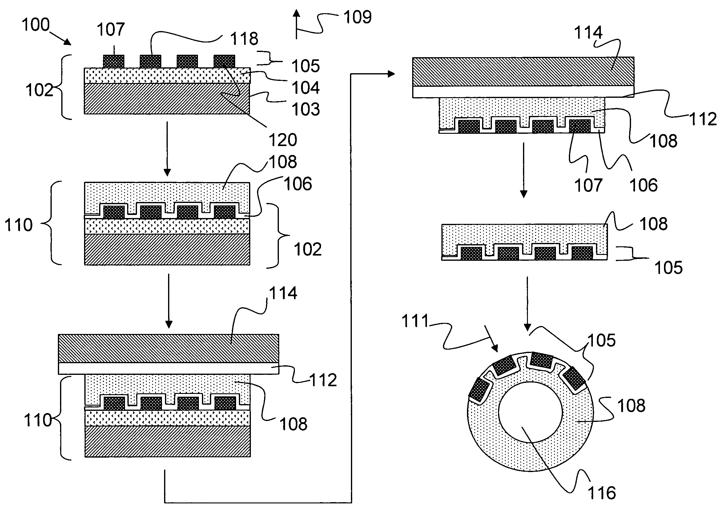
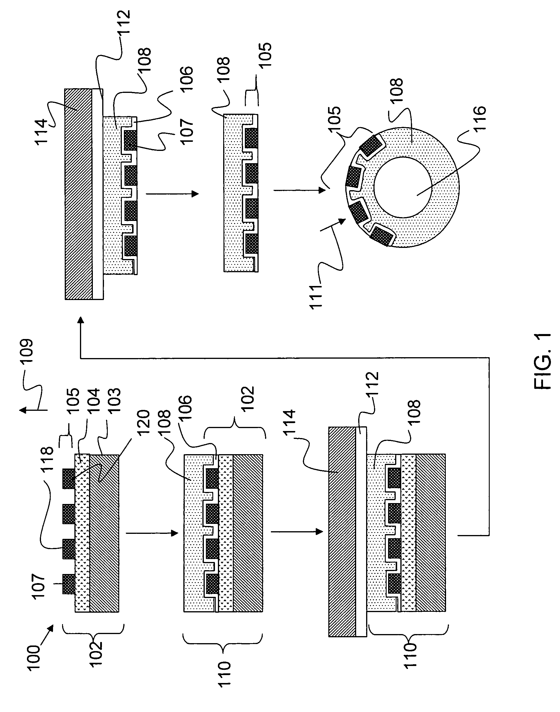
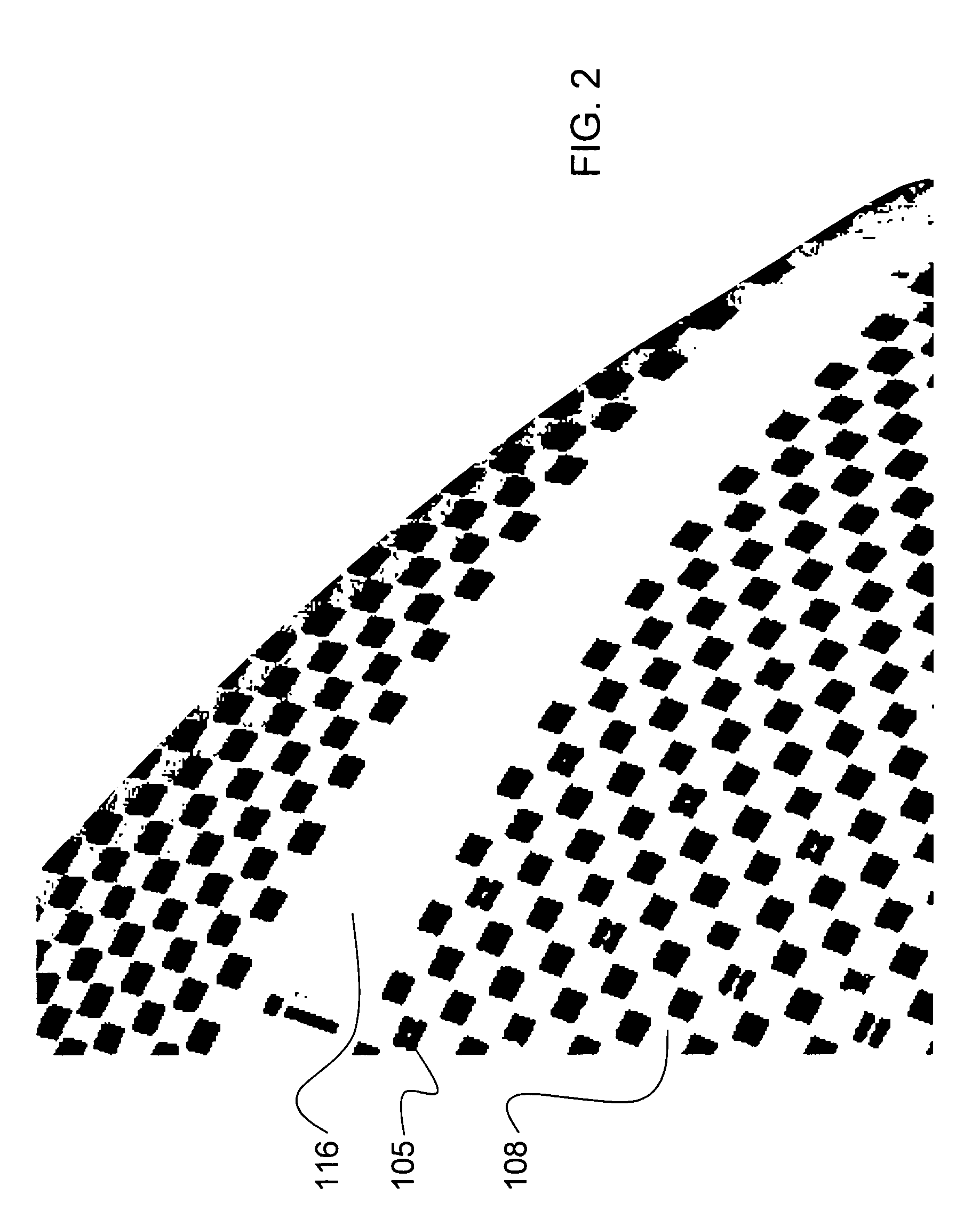
[0021]The present invention relates to micro-electronic array formation, and more particularly, to a method for forming a micro-electronic array that can conform its shape to an arbitrary three-dimensional shape. The following description is presented to enable one of ordinary skill in the art to make and use the invention and to incorporate it in the context of particular applications. Various modifications, as well as a variety of uses in different applications will be readily apparent to those skilled in the art, and the general principles defined herein may be applied to a wide range of embodiments. Thus, the present invention is not intended to be limited to the embodiments presented, but is to be accorded the widest scope consistent with the principles and novel features disclosed herein.

[0022]In the following detailed description, numerous specific details are set forth in order to provide a more thorough understanding of the present invention. However, it will be apparent to...


PUM

PropertyMeasurementUnit
diameteraaaaaaaaaa
diameteraaaaaaaaaa
temperatureaaaaaaaaaa

Abstract

Described is a method for conforming electronics to arbitrary shapes. The method comprises acts of forming a device structure to have a growth substrate, an etch stop layer affixed with the growth substrate, and a micro-electronic array. The micro-electronic array comprises a plurality of components atop the etch stop layer. The micro-electronic array is thereafter embedded into a shrinkable layer. The shrinkable layer is then mounted onto a handle wafer that includes a layer of adhering film with the shrinkable layer being pressed into the layer of adhering film. The growth substrate and the etch stop layer are thereafter removed. The adhering film is then dissolved to demount the micro-electronic array and shrinkable layer. Finally, the shrinkable layer is shrunk to conform the micro-electronic array to a three-dimensional shape, with the growth orientation flipped such that metal interconnects may be made to both the top and bottom of the chip.

Description

BACKGROUND OF THE INVENTION[0001](1) Field of Invention[0002]The present invention relates to microelectronic array formation, and more particularly, to a method for forming a microelectronic array that can conform its shape to an arbitrary three-dimensional shape.[0003](2) Description of Related Art[0004]Electronics and / or semiconductors are typically formed as flat wafers. In some circumstances, it may be desirable to form a semiconductor as a curved structure. However, current semiconductor technology is limited in its ability to form curved structures containing high densities of active components. There are known techniques that employ simple bending procedures of a thinned crystalline material, or segmenting the structure into sub-arrays to allow for curving of the arrays. By way of example, Dr. James Gregory of the Massachusetts Institute of Technology (MIT) Lincoln Laboratory (LL), used a bending procedure to bend thin charge coupled device (CCD) arrays (details given below)...

Claims


Application Information

Patent Timeline
Patent Type & Authority Patents(United States)
IPC IPC(8): G02F1/03H01L23/34
CPCH01L21/6835H01L21/6836H01L23/4985H01L23/5389H01L25/065H01L25/50H01L27/14812H01L2924/1305H01L24/82H01L29/78603H01L2221/68327H01L2221/6835H01L2221/68363H01L2221/68368H01L2924/01079H01L2924/14H01L2924/00
Inventor PATTERSON, PAMELAHUNTER, ANDYSHUM, ANGELABREWER, PETER DAVID
Owner HRL LAB
Why Eureka
Try Eureka