Semiconductor laser device, method for fabricating the same, and optical disk apparatus

a semiconductor laser and laser device technology, applied in semiconductor lasers, optical resonator shapes and construction, optical beam sources, etc., can solve the problems of reducing device reliability, meeting the demand of increasing laser device output power, dioxide and titanium oxide films, etc., to increase output power, reduce wavelength, and improve the effect of semiconductor laser devices

Inactive Publication Date: 2007-11-06
PANASONIC CORP
View PDF24 Cites 4 Cited by
  • Summary
  • Abstract
  • Description
  • Claims
  • Application Information

AI Technical Summary

Benefits of technology

[0017]It is therefore an object of the present invention to solve these problems of the prior art and obtain an end facet reflective film that can meet the demand of increasing the output power, or decreasing the wavelength, of semiconductor laser devices.
[0020]In the first semiconductor laser device, the reflective film formed on the end facet of the resonant cavity contains, for example, niobium oxide having a light absorption coefficient smaller than that of titanium oxide. Thus, a smaller quantity of laser light is absorbed thereto compared to titanium oxide, and a rise in temperature of the reflective film is suppressed. As a result, it is possible to prevent the crystal structure of the semiconductor layers from deteriorating in the vicinity of the end facet of the resonant cavity, and the laser device can increase its output power or decrease its wavelength.
[0022]The second semiconductor laser device achieves the same effects as those of the first semiconductor laser device. In addition, the reflective film is made up of the high-refractive-index film of niobium oxide and the first dielectric layer with a refractive index smaller than that of niobium oxide. Thus, the reflectance can be increased as intended.
[0024]In the third semiconductor laser device, the reflective films of the second semiconductor laser device are stacked a number of times. Accordingly, the reflectance further increases. Moreover, in a laser device with an oscillation wavelength belonging to the red part of the spectrum, a dielectric with a refractive index greater than that of niobium oxide, e.g., titanium oxide, may be used for the second dielectric layer located on the other side of the reflective film that is opposite to the end facet of the resonant cavity, i.e., the outermost second dielectric layer. Then, it is possible to increase the reflectance of the reflective film because the absorption coefficient of titanium oxide is not so high, either, in the red part of the spectrum.

Problems solved by technology

Due to a rise in temperature caused by this light absorption, the crystallinity of the laser device in the vicinity of the resonant cavity end facet thereof deteriorates, and thus the reliability of the device declines.
However, there is a problem that neither the known end facet reflective film as a stack of silicon dioxide and amorphous silicon films for the infrared or red-light-emitting semiconductor laser device with an oscillation wavelength of about 780 nm nor the known end facet reflective film as a stack of silicon dioxide and titanium oxide films for the red-light-emitting semiconductor laser device with an oscillation wavelength of about 650 nm can meet the demand of increasing the output power of laser devices.
Further, there is another problem that the end facet reflective film as a stack of silicon dioxide and titanium oxide films for the violet-light-emitting semiconductor laser device with an oscillation wavelength of about 400 nm cannot meet the demand of decreasing the wavelength of laser devices.
This is because the light, emitted from these semiconductor laser device, is absorbed into the high-refractive-index film at an insufficiently small coefficient.
As a result, the crystallinity of the semiconductor laser devices deteriorates especially in part of the active region near the resonant cavity end facet thereof.
In the same way, if a laser device should have an oscillation wavelength as short as 400 nm or less, it is difficult to operate the device properly with a known end facet reflective film as a stacked structure including silicon dioxide.

Method used


Image

  • Semiconductor laser device, method for fabricating the same, and optical disk apparatus
  • Semiconductor laser device, method for fabricating the same, and optical disk apparatus
  • Semiconductor laser device, method for fabricating the same, and optical disk apparatus

Examples


embodiment 1

[0041]A first embodiment of the present invention will be described with reference to the drawings.

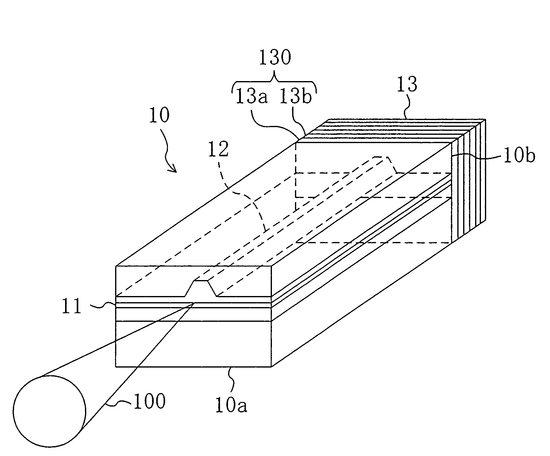
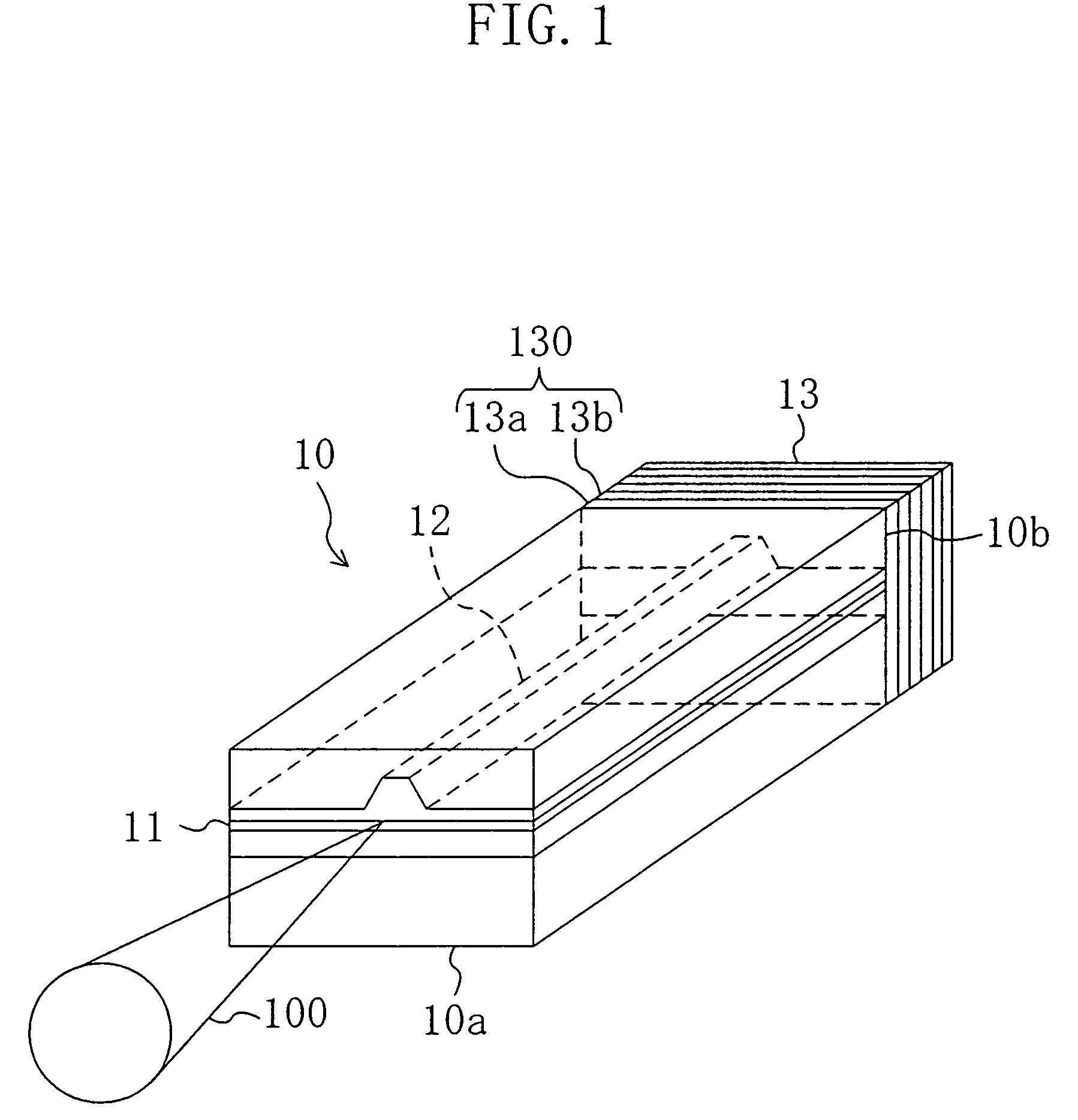
[0042]FIG. 1 shows a semiconductor laser device according to the first embodiment of the present invention, which is a violet-light-emitting semiconductor laser device with an oscillation wavelength of about 400 nm.

[0043]As shown in FIG. 1, the semiconductor laser device 10 includes a resonant cavity 12 in which a quantum well active layer 11 made up of barrier layers of gallium nitride (GaN), for example, and well layers of indium gallium nitride (InGaN), for example, is vertically sandwiched between at least light guide layers of n- and p-type aluminum gallium nitride (AlGaN), for example.

[0044]An end facet reflective film 13 is formed on a reflective end facet 10b opposite to a light-emitting end facet 10a for laser light 100 in the resonant cavity 12.

[0045]The end facet reflective film 13 has a structure including a plurality of unit reflective films 130, each of which is made up o...

embodiment 2

[0076]Hereinafter, a second embodiment of the present invention will be described.

[0077]In the first embodiment described above, niobium oxide is used for the high-refractive-index film that can cope with the demand for decreased wavelength. On the other hand, the second embodiment is adapted to cope with the demand for increasing the output power of a semiconductor laser device with a long oscillation wavelength covering infrared to red parts of the spectrum.

[0078]For example, a laser device for a 16×CD-R, on which data can be written only once sixteen times faster than normal speed, should have an optical output of 150 mW in a pulsed drive mode at a duty cycle of 50% and 110 mw in a CW drive mode. Thus, the known end facet reflective film, which is made up of a low-refractive-index film of silicon dioxide and a high-refractive-index film of amorphous silicon, cannot attain sufficient reliability.

[0079]In view of this, in the second embodiment, first and second dielectric layers fo...

embodiment 3

[0090]Hereinafter, a third embodiment of the present invention will be described with reference to the drawing.

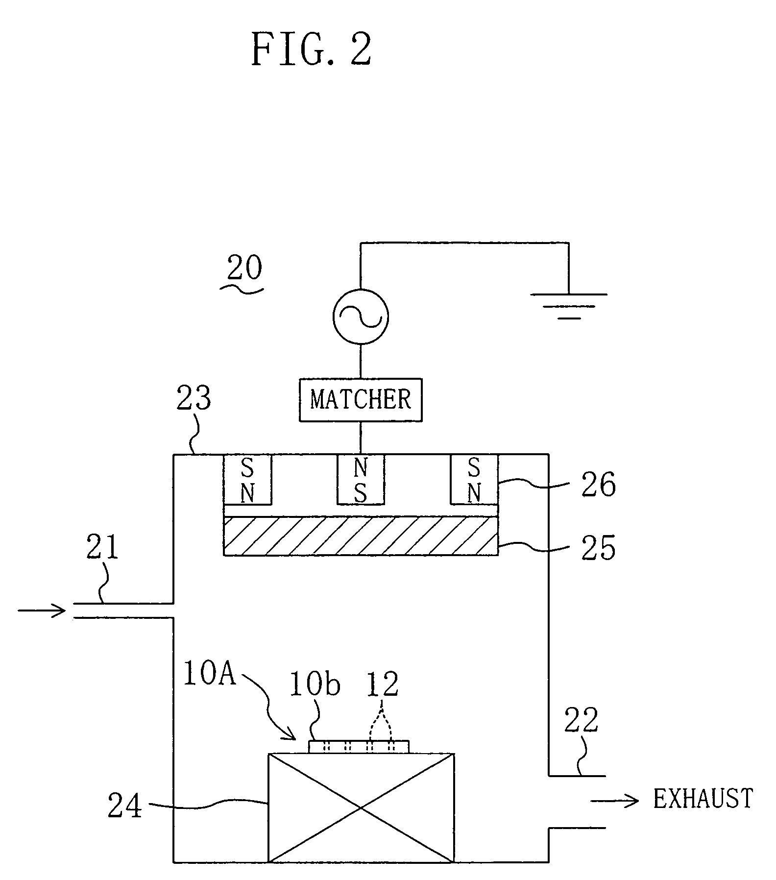
[0091]FIG. 6 schematically shows an arrangement for an optical disk apparatus according to the third embodiment of the present invention. In FIG. 6, in the optical disk apparatus according to the third embodiment, the semiconductor laser device of the present invention, i.e., the violet-light-emitting semiconductor laser device according to the first embodiment, is used as a light-emitter 41 of the optical disk apparatus.

[0092]As shown in FIG. 6, in the optical disk apparatus, the light-emitting end facet of the semiconductor laser device as the light-emitter 41 and the data-retaining surface of the optical disk 50 as a storage medium, on which desired data has been recorded, are disposed to face each other. A condensing optical system 40 is placed between the light-emitter 41 and the optical disk 50.

[0093]In the condensing optical system 40, collimator lens 42 that changes...


PUM

PropertyMeasurementUnit
absorption coefficientaaaaaaaaaa
reflectanceaaaaaaaaaa
absorption coefficientaaaaaaaaaa

Abstract

A semiconductor laser device (10) includes a resonant cavity (12) in which a quantum well active layer (11) made up of barrier layers of gallium nitride and well layers of indium gallium nitride is vertically sandwiched between at least light guide layers of n- and p-type aluminum gallium nitride. An end facet reflective film (13) is formed on a reflective end facet (10b) opposite to a light-emitting end facet (10a) in the resonant cavity (12). The end facet reflective film (13) has a structure including a plurality of unit reflective films (130), each of which is made up of a low-refractive-index film (13a) of silicon dioxide and a high-refractive-index film (13b) of niobium oxide. The low-and high-refractive-index films are deposited in this order on the end facet of the resonant cavity (12).

Description

[0001]This application is a continuation of application Ser. No. 09 / 890,095 filed Jul. 27, 2001, now U.S. Pat. No. 6,798,811 which is a 371 application of PCT / JP00 / 08461, filed Nov. 29, 2000.[0002]Priority of application Ser. No. 11-339195 filed on Nov. 29, 1999, in Japan is claimed under 35 USC 119. The certified priority document was received by the International Bureau of WIPO on Jan. 29, 2001.TECHNICAL FIELD[0003]The present invention relates to a semiconductor laser device expectedly applicable to the field of optical information processing, a method for fabricating the device, and an optical disk apparatus in which the semiconductor laser device is used for its light-emitting portion.BACKGROUND ART[0004]In general, an end facet reflective film is provided on an end facet of the laser light resonant cavity of a semiconductor laser device. Particularly, a reflective end facet, which is a rear end facet opposite to the laser-light-emitting facet, should have a high reflectance. T...

Claims


Application Information

Patent Timeline
Patent Type & Authority Patents(United States)
IPC IPC(8): H01S5/00G11B7/125H01S5/028H01S5/20H01S5/223H01S5/343
CPCB82Y20/00G11B7/127H01S5/34333H01S5/028H01S5/2004H01S5/2231
Inventor SUGAHARA, GAKUKIDOGUCHI, ISAOMIYANAGA, RYOKOSUZUKI, MASAKATSUKUME, MASAHIROBAN, YUSABUROHIRAYAMA, FUKUKAZU
Owner PANASONIC CORP
Why Eureka
Try Eureka