High bandwidth memory management using multi-bank DRAM devices

a memory management and multi-bank technology, applied in the direction of memory adressing/allocation/relocation, instruments, computing, etc., can solve the problems of reducing the available bandwidth, overlapping bank operations are lost, and the benefits of hiding access latencies behind multiples, so as to maximize the performance of dram operations and avoid the incumbent pre-charge latency associated with the effect of latency

Inactive Publication Date: 2007-11-13
CISCO TECH INC
View PDF8 Cites 51 Cited by
  • Summary
  • Abstract
  • Description
  • Claims
  • Application Information

AI Technical Summary

Benefits of technology

[0014]One example of a benefit provided by the various embodiments of the invention is achieving very high data storage and retrieval bandwidths, particularly with very short bursts or no bursts. Storing data segments of a data word in parallel into memory banks across a plurality of DRAM devices maximizes the performance of DRAM operations by minimizing the likelihood that a long sequence of accesses will be directed at a single bank, thereby avoiding the incumbent pre-charge latency associated with such a long sequence of accesses at a single bank.

Problems solved by technology

Wide data interfaces make it impractical to achieve data bursts long enough to make the gaps between bursts insignificant.
Hence, short random accesses suffer from the precharge latency overhead on each cycle thereby significantly reducing the available bandwidth.
However, if a sequence of DRAM accesses were all addressed to the same bank, the benefits of hiding the access latencies behind multiple, overlapping bank operations is lost.

Method used


Image

  • High bandwidth memory management using multi-bank DRAM devices
  • High bandwidth memory management using multi-bank DRAM devices
  • High bandwidth memory management using multi-bank DRAM devices

Examples


Embodiment Construction

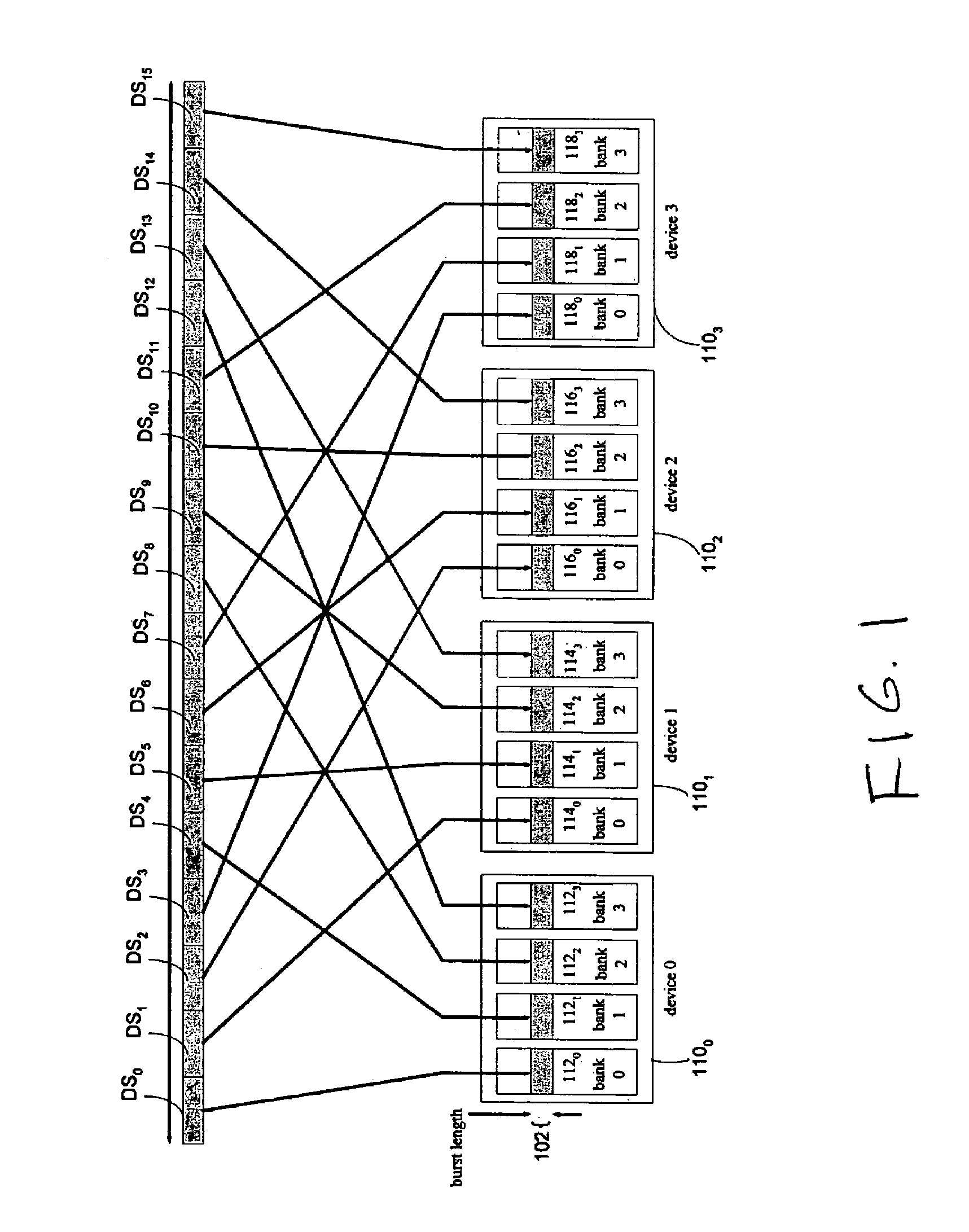
[0024]FIG. 1 illustrates an example 100 of a striping data segments of a data word in parallel in banks across a plurality of DRAM devices in accordance with an embodiment of the present invention. In this example, there are four DRAM devices, 1100, 1101, 1102, 1103, each with a corresponding set of four banks, 1120, 1121, 1122, 1123, 1140, 1141, 1142, 1143, 1160, 1161, 1162, 1163, and 1180, 1181, 1182, 1183. Each bank has the same data width and data storage depth characteristics, and each DRAM device has the same number of banks.

[0025]A data word can range in width from a single byte to several hundred bytes or several thousand bytes. In one embodiment in accordance with the present invention as illustrated in FIG. 1, a maximum word width is chosen so as to bound system behavior. In this example, the data word is separated into a number of data segments. In this example, the data segments, a representative example of which is DS1, are of an equal, fixed size. An objective of this ...


PUM


Abstract

The disclosure describes implementations for accessing in parallel a plurality of banks across a plurality of DRAM devices. These implementations are suited for operation within a parallel packet processor. A data word in partitioned into data segments which are stored in the plurality of banks in accordance with an access scheme that hides pre-charging of rows behind data transfers. A storage distribution control module is communicatively coupled to a memory comprising a plurality of storage request queues, and a retrieval control module is communicatively coupled to a memory comprising a plurality of retrieval request queues. In one example, each request queue may be implemented as a first-in-first-out (FIFO) memory buffer. The plurality of storage request queues are subdivided into sets as are the plurality of retrieval queues. Each is set is associated with a respective DRAM device. A scheduler for each respective DRAM device schedules data transfer between its respective storage queue set and the DRAM device and between its retrieval queue set and the DRAM device independently of the scheduling of the other devices, but based on a shared criteria for queue service.

Description

CROSS-REFERENCE TO RELATED APPLICATION[0001]This application claims the benefit of priority under 35 U.S.C. § 119(e) to U.S. provisional patent application No. 60 / 432,528, filed on Dec. 10, 2002, entitled “System and Method for High Bandwidth Memory Management,” which is hereby incorporated by reference.FIELD OF INVENTION[0002]The present invention relates to managing access to dynamic random access memory (DRAM) devices, particularly in a parallel packet processor in a data network.BACKGROUND[0003]Dynamic random access memories (DRAMs) provide tremendous benefits in terms of storage density and are capable of transferring large amounts of data very quickly if that data is carefully organized into long bursts of consecutive data transfers to and from adjacent memory locations. Since the data interfaces of these DRAMs are limited in their per-pin bandwidth, high bandwidths are achieved through very wide data interfaces.[0004]Certain applications, such as network communications involv...

Claims


Application Information

Patent Timeline
Patent Type & Authority Patents(United States)
IPC IPC(8): G06F12/00
CPCG06F12/06
Inventor YARLAGADDA, RAMESHDESAI, SHWETALDEVANAGONDI, HARISH R.
Owner CISCO TECH INC
Why Eureka
Try Eureka