Method of fabricating a mask ROM

a mask rom and fabrication method technology, applied in the direction of semiconductor devices, basic electric elements, electrical equipment, etc., can solve the problems of difficulty in appropriately implementing the junction depth and line width in the aspect of channel margin, and achieve the effect of enhancing resistance characteristics and minimizing device siz

Inactive Publication Date: 2007-11-27
DONGBU HITEK CO LTD
View PDF13 Cites 0 Cited by
  • Summary
  • Abstract
  • Description
  • Claims
  • Application Information

AI Technical Summary

Benefits of technology

[0021]An advantage of the present invention is that it provides a mask ROM and fabricating method thereof, in which a bit line is formed of a conductive material such as polysilicon, by which a device size can be minimized, and by which resistance characteristics are enhanced.
[0022]Additional advantages and features of the invention will be set forth in part in the description which follows, and will become apparent from the description, or may be learned by practice of the invention. These and other advantages of the invention may be realized and attained by the structure particularly pointed out in the written description and claims hereof as well as the appended drawings.
[0023]To achieve these and other advantages and in accordance with the purpose of the invention, as embodied and broadly described herein, a mask ROM present invention includes a semiconductor substrate divided into a device isolation area and an active area, an impurity region on a prescribed portion in the active area, a first electrode layer pattern on the semiconductor substrate to correspond to a region except the impurity region, a second electrode layer pattern on the impurity region, and a third electrode layer pattern over the semiconductor substrate including the first and second electrode patterns.
[0024]In another aspect of the present invention, a method of fabricating a mask ROM includes the steps of forming a gate insulating layer on a semiconductor substrate divided into a device isolation area and an active area, depositing a first electrode layer, a first dielectric layer and a second dielectric layer on the gate insulating layer, forming a first electrode layer pattern, a first dielectric layer pattern and a second dielectric layer pattern, each having a same width, on a predetermined area of the gate insulating by selectively removing the first electrode layer, the first dielectric layer and the second dielectric layer, forming the impurity region by implanting impurities into an area except the first electrode layer pattern, forming a second electrode layer pattern on the impurity region, forming an oxide layer by oxidizing a surface of the second electrode layer pattern, removing the first and second dielectric layer patterns, forming a third electrode layer over the semiconductor substrate including the first and second electrode layer patterns, planarizing the third electrode layer, forming a word line by selectively removing the first and third electrode layers, and filling a gap between the word lines with an oxide layer.

Problems solved by technology

Yet, as a cell size is reduced, it is difficult to appropriately implement the junction depth and line width in aspect of channel margin.

Method used


Image

  • Method of fabricating a mask ROM
  • Method of fabricating a mask ROM
  • Method of fabricating a mask ROM

Examples


Embodiment Construction

[0032]Reference will now be made in detail to exemplary embodiments of the present invention, examples of which are illustrated in the accompanying drawings. Wherever possible, the same reference numbers will be used throughout the drawings to refer to the same or like parts.

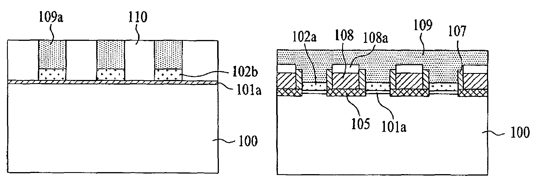
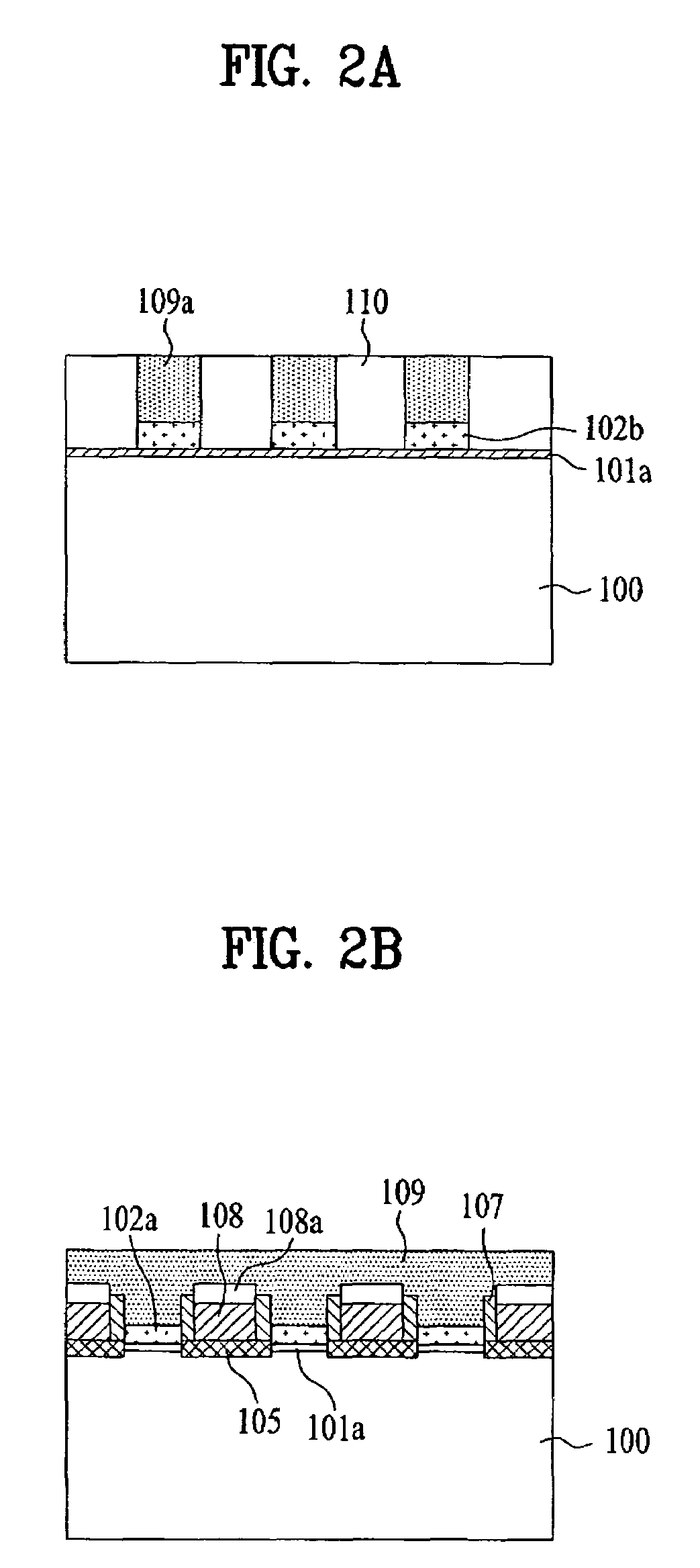
[0033]FIG. 2A is a cross-sectional diagram of a mask ROM according to an exemplary embodiment of the present invention in a bit line direction and FIG. 2B is a cross-sectional diagram of a mask ROM according to an exemplary embodiment of the present invention in a word line direction.

[0034]Referring to FIG. 2A and FIG. 2B, a mask ROM according to an exemplary embodiment of the present invention includes a semiconductor substrate 100 having a device isolation layer (not shown in the drawings) and an active area defined thereon, a BN (buried N doped) impurity region 105 formed on a prescribed region of the active area, a second electrode layer pattern 108 formed on the impurity region 105 to have a prescribed heig...


PUM

PropertyMeasurementUnit
voltageaaaaaaaaaa
widthaaaaaaaaaa
semiconductoraaaaaaaaaa

Abstract

A mask ROM and fabrication method thereof are disclosed, in which a bit line is formed of a conductive material such as polysilicon, by which a device size can be minimized, and by which resistance characteristics are enhanced.

Description

CROSS REFERENCE TO RELATED APPLICATION[0001]This application claims the benefit of the Korean Patent Application No. P2004-0116148, filed on Dec. 30, 2004, which is hereby incorporated by reference for all purposes as if fully set forth herein.BACKGROUND OF THE INVENTION[0002]1. Field of the Invention[0003]The present invention relates to a semiconductor device, and more particularly, to a mask ROM and fabrication method thereof. Although the present invention is suitable for a wide scope of applications, it is particularly suitable for forming a bit line of a conductive material such as polysilicon to minimize device size and to enhance resistance characteristics.[0004]2. Discussion of the Related Art[0005]Typically, a flat ROM device is named after its structure. The name of the device is attributed to a fact that a step difference of a shape of bit and word lines is smaller than that of another memory device. A mask ROM is the name for specific coding selectively performed to set...

Claims


Application Information

Patent Timeline
Patent Type & Authority Patents(United States)
IPC IPC(8): H01L21/336
CPCH01L27/11253H01L27/112H10B20/38H10B20/00
Inventor KIM, HEUNG JIN
Owner DONGBU HITEK CO LTD
Why Eureka
Try Eureka