Supercharge Your Innovation With Domain-Expert AI Agents!

On-chip high frequency power supply noise sensor

a high-frequency power supply and noise sensor technology, applied in the direction of noise figure or signal-to-noise ratio measurement, instruments, measurement devices, etc., can solve problems such as chip damage, chip function error, and chip damag

Inactive Publication Date: 2007-11-27
INT BUSINESS MASCH CORP
View PDF5 Cites 14 Cited by
  • Summary
  • Abstract
  • Description
  • Claims
  • Application Information

AI Technical Summary

Benefits of technology

The invention provides an on-chip power supply noise detector that can be made using standard CMOS process technology. The detector directly senses power supply noise, without the need for calibration. It can be tuned to respond only to noise in a specific frequency range that could cause damage or errors. The detector uses a single power input from the power supply, making it placement flexible on the chip.

Problems solved by technology

An undetected noise signal introduced via the power supply to a processor, memory, or other integrated circuit chip, can damage the chip and / or cause an error in the chip function.
As pointed out above, if undetected, such noise signals can damage the chip and / or cause an undetected error in the chip's operation.

Method used


Image

  • On-chip high frequency power supply noise sensor
  • On-chip high frequency power supply noise sensor
  • On-chip high frequency power supply noise sensor

Examples


Embodiment Construction

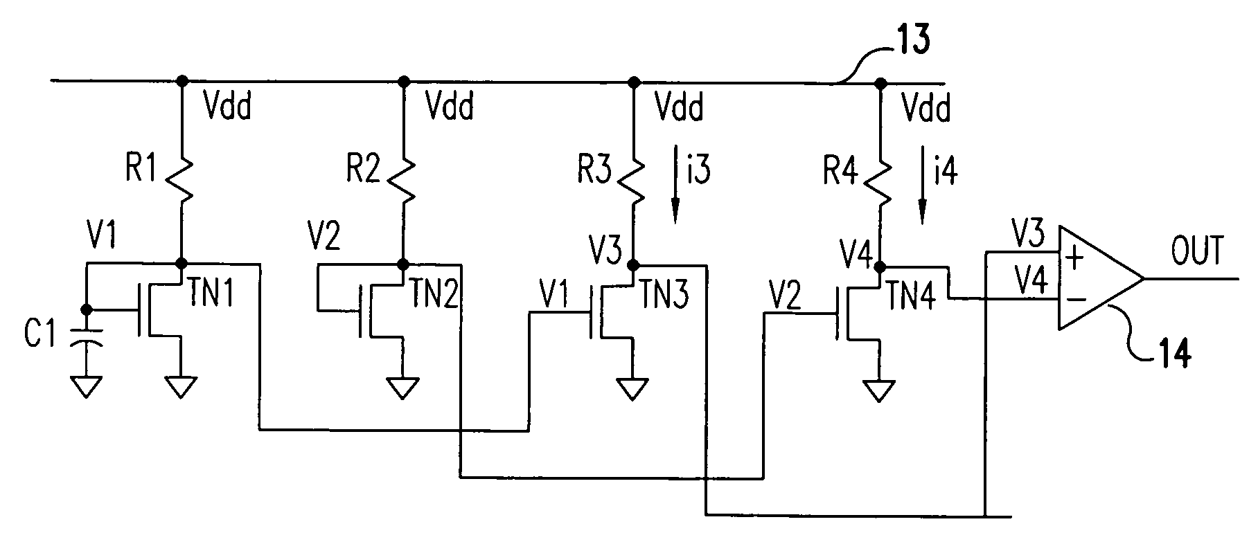
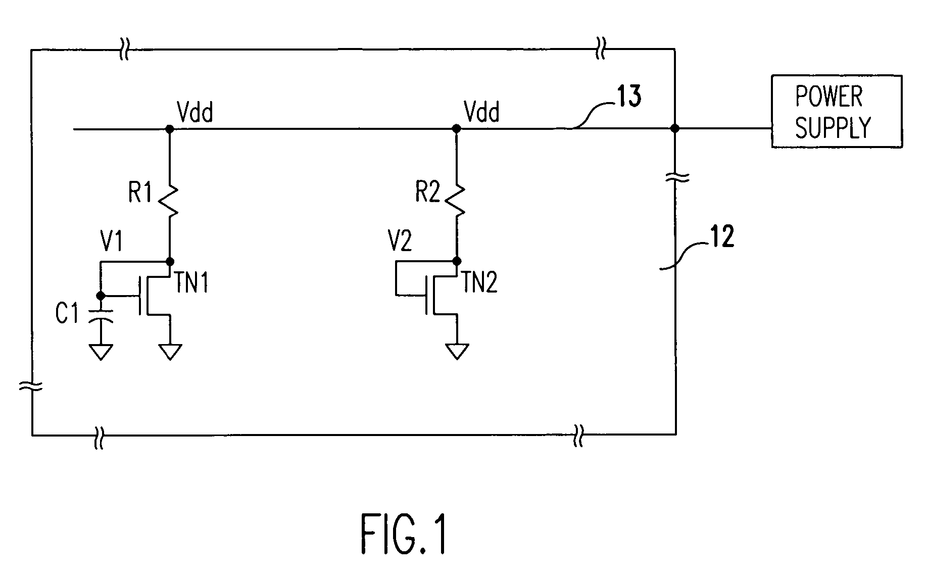
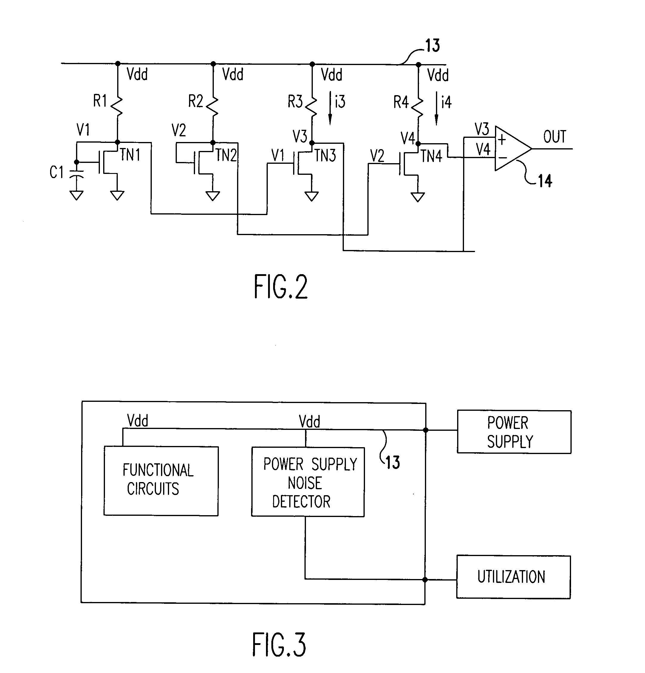
[0014]Referring now to FIG. 1 of the drawings, a pair of CMOS FETs TN1 and TN2 and their associated circuitry is formed on chip 12, preferably in the same process as used to form the functional components on the chip. The transistors TN1 and TN2 are connected each as a simple current generator, with resistors R1 and R2 connected to voltage Vdd on the chip's internal power supply bus 13. The value of TN1 and TN2 and the resistance of R1 and R2 are the same. The drain of each transistor TN1 and TN2 is connected to its gate so that the current in each is largely dependent on the power supply voltage Vdd. A capacitor C1 couples the gate of TN1 to common, with the capacitor C1 acting as a low pass filter where the resistance of the filter time constant is given by the inverse transconductance of transistor TN1 in parallel with the resistor R1. The current through TN2 will track changes in the power supply voltage Vdd introduced via bus 13 substantially instantaneously while the current t...


PUM


Abstract

The on-chip power supply noise sensor detects high frequency overshoots and undershoots of the power supply voltage. By creating two identical current sources and attaching a time constant circuit to only one, the high frequency transient behavior differs while the low frequency behavior is equivalent. By comparing these currents, the magnitude of very high frequency power supply noise can be sensed and used to either set latches or add to a digital counter. This has the advantage of directly sensing the power supply noise in a manner that does not require calibration. Also, since the sensor requires only one power supply, it can be used anywhere on a chip. Finally, it filters out any lower frequency noise that is not interesting to the circuit designer and can be tuned to detect down to whatever frequency is needed.

Description

BACKGROUND OF THE INVENTION[0001]1. Field of the Invention[0002]This invention relates to an improved on-chip detector of noise on the power supply input to the chip, and more particularly to a detector that can respond to high frequency, low magnitude noise levels and can be implemented with CMOS process technology.[0003]2. Description of Background[0004]An undetected noise signal introduced via the power supply to a processor, memory, or other integrated circuit chip, can damage the chip and / or cause an error in the chip function. A typical power supply may include circuits to regulate the power supply output in order to minimize and suppress noise in the power supplied to the chip that would take the power supply voltage out of the range permitted by the chip design. Notwithstanding such power supply regulation, noise, particularly high frequency noise signals riding on the dc power supply voltage, can be coupled to the chip. As pointed out above, if undetected, such noise signal...

Claims


Application Information

Patent Timeline
Patent Type & Authority Patents(United States)
IPC IPC(8): G05F5/00H02J1/02
CPCG01R19/16552H03K5/08G01R29/26
Inventor DREPS, DANIEL M.KIM, SEONGWONSPERLING, MICHAEL A.
Owner INT BUSINESS MASCH CORP
Features
  • R&D
  • Intellectual Property
  • Life Sciences
  • Materials
  • Tech Scout
  • Unparalleled Data Quality
  • Higher Quality Content
  • 60% Fewer Hallucinations
Learn More