Supercharge Your Innovation With Domain-Expert AI Agents!

Formation of metal-insulator-metal capacitor simultaneously with aluminum metal wiring level using a hardmask

a metal-insulator and capacitor technology, applied in the direction of fixed capacitors, fixed capacitor details, fixed capacitor terminals, etc., can solve the problems of undesirable eroding (rounded) corners of the upper plate, undesirable increase in wiring pitch, and less attractive and expensive technology, so as to reduce process complexity and cost, improve protection, and thin resist

Inactive Publication Date: 2007-11-27
GLOBALFOUNDRIES INC
View PDF14 Cites 10 Cited by
  • Summary
  • Abstract
  • Description
  • Claims
  • Application Information

AI Technical Summary

Benefits of technology

[0009]This etching process simultaneously patterns lower capacitor plates and wiring patterns in the lower conductor layer. Further, the etching process can comprise a multi-step etching process where different etches are used to pattern one or more of the hardmask, the upper conductor, the dielectric layer, the etchstop, the lower conductor, etc. The hardmask protects the upper conductor layer from corner rounding during the etching process.
[0014]Further, because the invention uses a hardmask, a much thinner photoresist can be used to pattern the hardmask and underlying conductor layers. This allows the invention to form much smaller features than that could be formed with a thicker photoresist. For example, the invention allows the spacing between wires in the wiring pattern to be as small as approximately one-half the height of the upper capacitor plate.
[0015]Therefore, the invention uses a hardmask to simultaneously pattern the bottom plate of the MIMCap and wiring level and can use a thinner resist to pattern the dielectric hardmask to the desired fine pitch. The invention uses the residual resist from the hardmask patterning to pattern the underlying conductive layer because the hardmask provides better protection for MIMCap. Further, the invention integrates an etchstop with the hardmask to further reduce process complexity and cost. Thus, the invention simultaneously patterns large structures with significant topography and very fine pitch structures, which was not possible prior to the invention.

Problems solved by technology

However, the photoresist can sometimes be too thin at the corners of the upper plate, which causes the corners of the upper plate to be undesirably eroded (rounded) during the patterning of the underlying conductive layer.
However, as the photoresist becomes thicker, the spacing between structures (capacitors, adjacent wiring, etc.) that can be patterned by the thicker photoresist increases, which undesirably increases the pitch of the wiring.
This necessitates additional levels to compensate for loss in wirability, and makes the technology less attractive and more expensive.
However, this is also unattractive because it necessitates that there be a wider pitch level for designs which have MIMCaps, which again adds cost and complexity.

Method used


Image

  • Formation of metal-insulator-metal capacitor simultaneously with aluminum metal wiring level using a hardmask
  • Formation of metal-insulator-metal capacitor simultaneously with aluminum metal wiring level using a hardmask
  • Formation of metal-insulator-metal capacitor simultaneously with aluminum metal wiring level using a hardmask

Examples


Embodiment Construction

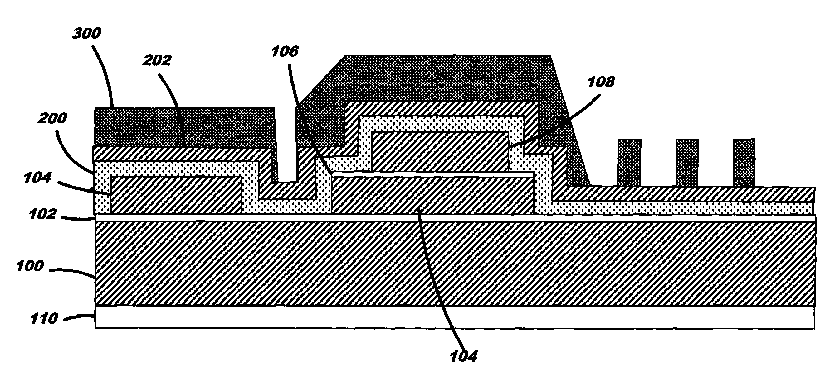
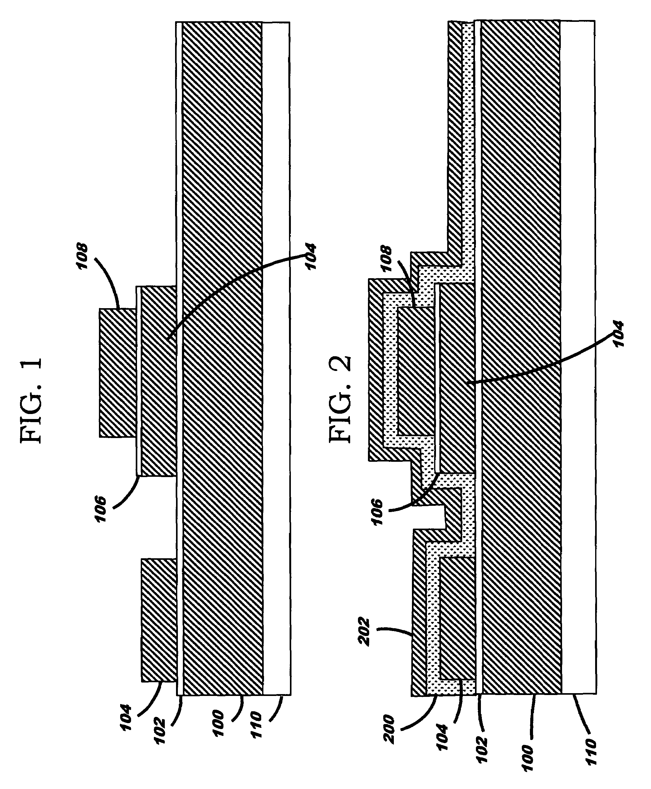
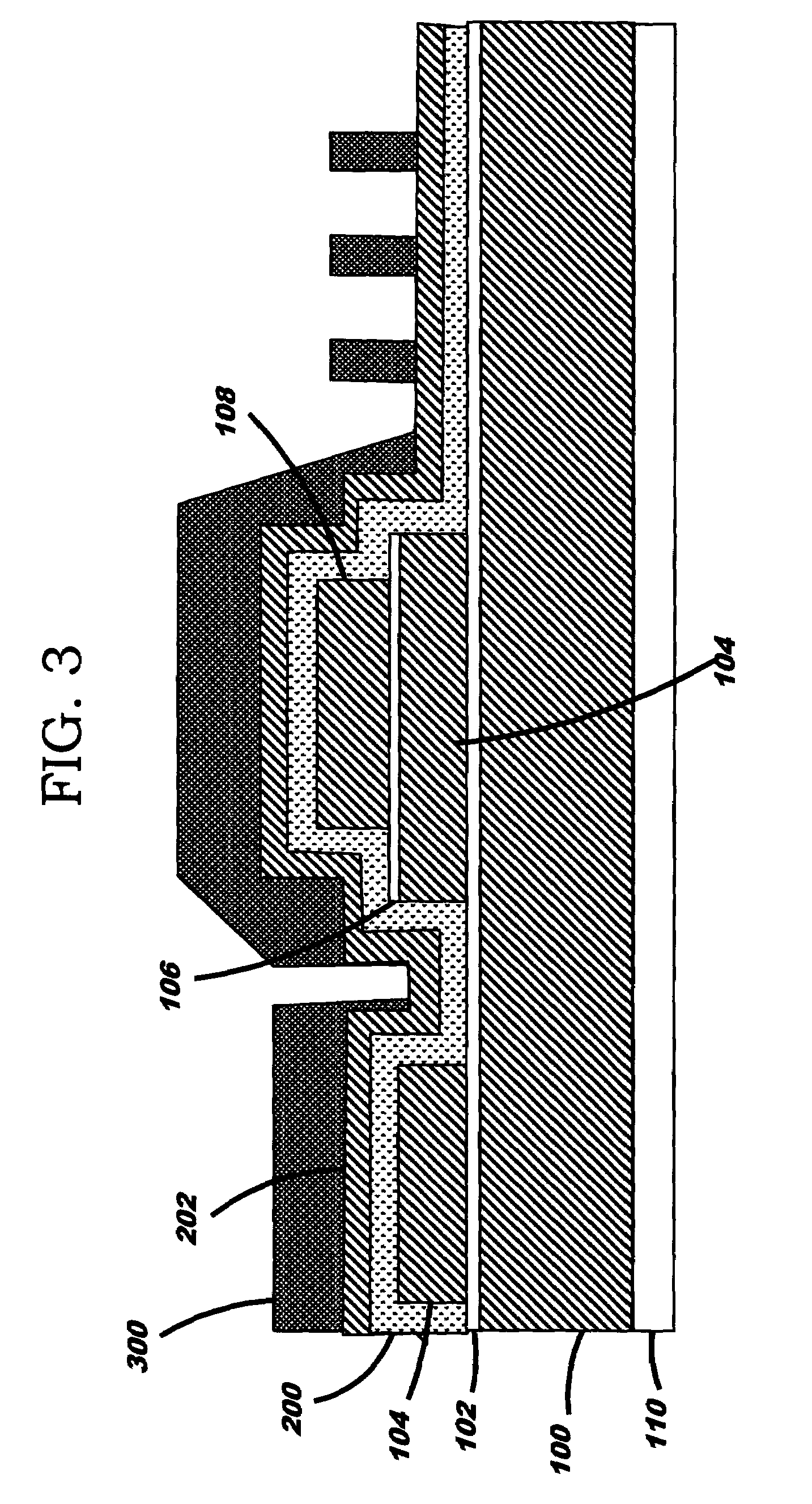
[0026]The present invention and the various features and advantageous details thereof are explained more fully with reference to the nonlimiting embodiments that are illustrated in the accompanying drawings and detailed in the following description. It should be noted that the features illustrated in the drawings are not necessarily drawn to scale. Descriptions of well-known components and processing techniques are omitted so as to not unnecessarily obscure the present invention. The examples used herein are intended merely to facilitate an understanding of ways in which the invention may be practiced and to further enable those of skill in the art to practice the invention. Accordingly, the examples should not be construed as limiting the scope of the invention.

[0027]As mentioned above, a MIMCap type of capacitor has a lower conductive plate and an upper conductive plate separated by a dielectric. Dual MIMCap have the same lower conductive plate, dielectric, and upper conductive pl...


PUM

PropertyMeasurementUnit
heightaaaaaaaaaa
structureaaaaaaaaaa
conductiveaaaaaaaaaa

Abstract

Disclosed is a method of fabricating a metal-insulator-metal (MIM) capacitor. In this method, a dielectric layer is formed above a lower conductor layer and an upper conductor layer is formed above the dielectric layer. The invention then forms an etch stop layer above the upper conductor layer and the dielectric layer, and forms a hardmask (silicon oxide hardmask, a silicon nitride hardmask, etc.) over the etch stop layer. Next, a photoresist is patterned above the hardmask, which allows the hardmask, the etch stop layer, the dielectric layer, and the lower conductor layer to be etched through the photoresist.

Description

BACKGROUND OF INVENTION[0001]1. Field of the Invention[0002]The present invention generally relates to a method of fabricating a metal-insulator-metal (MIM) capacitor, where a hardmask is formed over the capacitor and a photoresist is patterned above the hardmask, which allows the capacitor and corresponding wiring layer to be simultaneously etched through the photoresist, without damaging the upper plate of the capacitor.[0003]2. Description of the Related Art[0004]Capacitors are widely used in integrated circuit technology. One type of well-known capacitor is the metal-insulator-metal capacitor (MIMCap). This type of capacitor has a lower conductive plate and an upper conductive plate separated by a dielectric. When manufacturing metal-insulator-metal capacitors, the dielectric and the upper plate are patterned on a conductive layer. A photoresist is then formed over the dielectric and upper plate in order to pattern the conductive layer into the lower conductive plate. However, t...

Claims


Application Information

Patent Timeline
Patent Type & Authority Patents(United States)
IPC IPC(8): H01G4/38H01L21/02H01L21/20H01L21/8242H01L27/01H01L27/08
CPCH01L23/5223H01L27/016H01L27/0805H01L28/40Y10T29/49002H01L2924/0002H01L2924/00H10B99/00H10B12/00
Inventor COOLBAUGH, DOUGLAS D.ESHUN, EBENEZER E.FEILCHENFELD, NATALIE B.GAUTSCH, MICHAEL L.HE, ZHONG-XIANGMOON, MATTHEW D.RAMACHANDRAN, VIDHYAWATERHOUSE, BARBARA
Owner GLOBALFOUNDRIES INC
Features
  • R&D
  • Intellectual Property
  • Life Sciences
  • Materials
  • Tech Scout
  • Unparalleled Data Quality
  • Higher Quality Content
  • 60% Fewer Hallucinations
Learn More