Standard cell, standard cell library, semiconductor device, and placing method of the same

a technology of standard cell and semiconductor device, which is applied in the direction of solid-state devices, instruments, computer aided design, etc., can solve the problems of low level of area efficiency, reduced area efficiency, and reduced efficiency of insertion, so as to reduce the minimum area to be inserted, suppress the effect of increasing the area and reducing the area

Inactive Publication Date: 2007-11-27
SOCIONEXT INC
View PDF2 Cites 38 Cited by
  • Summary
  • Abstract
  • Description
  • Claims
  • Application Information

AI Technical Summary

Benefits of technology

[0013]An object of the present invention is to achieve a standard cell placement having a satisfactory level of area efficiency, in which a standard cell has a sufficient height so that the width in the traverse direction of an element, such as a transistor or the like, is not longer than the width in the height direction of the element, and an area for providing a well region can be obtained without an increase in area even when standard cells whose border lines between the N-well region and the P-well region have different heights are adjacent to each other.
[0014]To achieve this object, in the present invention, the shape of the border line between the N-well region and the P-well region is changed so that the border line height is converted at one or both ends of a standard cell to fit the border line height of another standard cell adjacent thereto, thereby causing all adjacent well regions to have the same type. Further, the standard cell height is set to be high. For example, a standard cell is designed so that a high-performance and large-size transistor is not longer in the traverse direction than in the height direction and the high-speed performance is exploited. Furthermore, by utilizing a gap region which occurs in a standard cell in which a small element is provided when the standard cell height is high, as a region for converting the border line height, the area efficiency is increased.

Problems solved by technology

However, in the case where standard cells have the same high height and the well border lines thereof have the same height, when a transistor having a low level of performance (i.e., a so-called small-size transistor) is realized, a useless region may occur and therefore the area efficiency may be reduced. FIG. 32 is a diagram illustrating a specific example of this situation, i.e., a standard cell which has a CMOS structure employing a small-size transistor and has a low level of area efficiency.
When the low-performance transistors are provided in the standard cell having the high cell height in this manner, a useless region corresponding to the interval W103 occurs and therefore the area efficiency is reduced.
When an attempt is made to provide a large-size transistor in a standard cell having a low height in this manner, the standard cell has a longer width in a traverse direction (perpendicular to the height direction) than in the height direction, and a gap region occurs at a border between P and N wells, resulting in a low level of area efficiency.
Thus, it is difficult to minimize the area of each standard cell.

Method used


Image

  • Standard cell, standard cell library, semiconductor device, and placing method of the same
  • Standard cell, standard cell library, semiconductor device, and placing method of the same
  • Standard cell, standard cell library, semiconductor device, and placing method of the same

Examples


first example

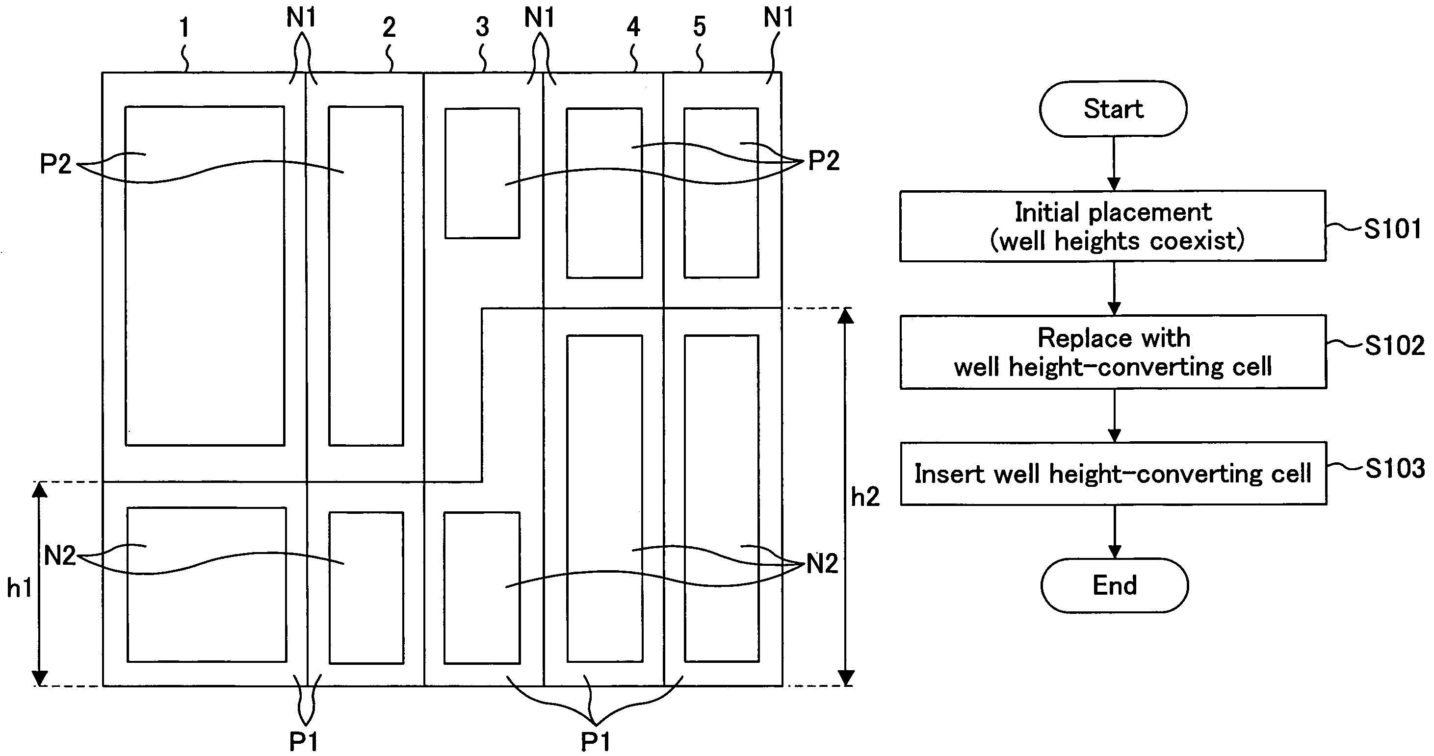
[0080]FIG. 1 is a standard cell placement diagram illustrating an exemplary layout of a standard cell semiconductor device according to a first example of the present invention. Note that standard cells indicated with the same reference numeral are identical to each other throughout the drawings in the first example or later.

[0081]In FIG. 1, 1 to 5 each indicate a standard cell. Each standard cell comprises an N-well region N1 (upper side) and a P-well region P1 (lower side). The N-well region N1 has a P-type diffusion region (P-type active region) P2 for forming a P-channel transistor, and the P-well region P1 has an N-type diffusion region (N-type active region) N2 for forming an N-channel transistor.

[0082]In the standard cells 1 to 5, a large-size transistor is realized by setting the height of the standard cell to be high without dividing into a plurality of standard cells using a parallel structure, thereby preventing a reduction in the area efficiency and a reduction in the cu...

second example

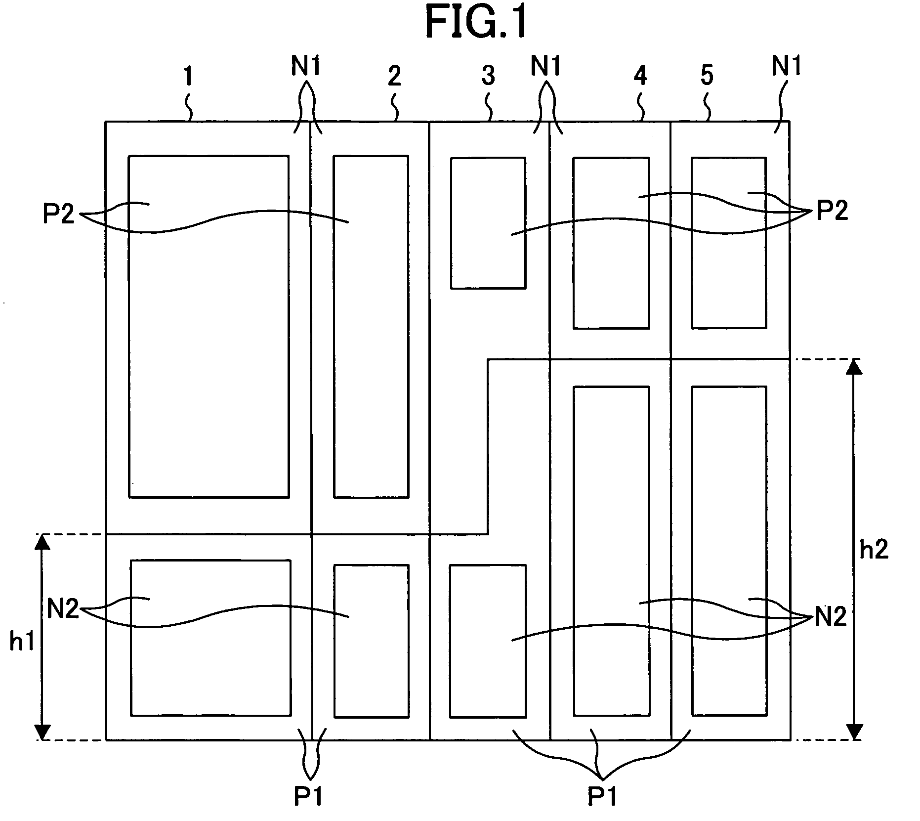
[0087]FIG. 2 is a standard cell placement diagram illustrating an exemplary layout of a standard cell semiconductor device according to a second example of the present invention.

[0088]Standard cells 1 and 2 are first standard cells in which a size of the P-channel transistor is larger than that of the N-channel transistor, a size of the P-type diffusion region P2 is larger than that of the N-type diffusion region N2, and the P-well region P1 has a height h1 (first height) at both ends thereof. Standard cells 4 and 5 are second standard cells in which a size of the N-channel transistor is larger than that of the P-channel transistor, a size of the N-type diffusion region N2 is larger than that of the P-type diffusion region P2, and the P-well region P1 has a height h2 (second height) which is different from h1, at both ends thereof. Standard cells 7 and 8 are fourth standard cells in which a size of the N-channel transistor is equal to that of the P-channel transistor, and the P-well...

third example

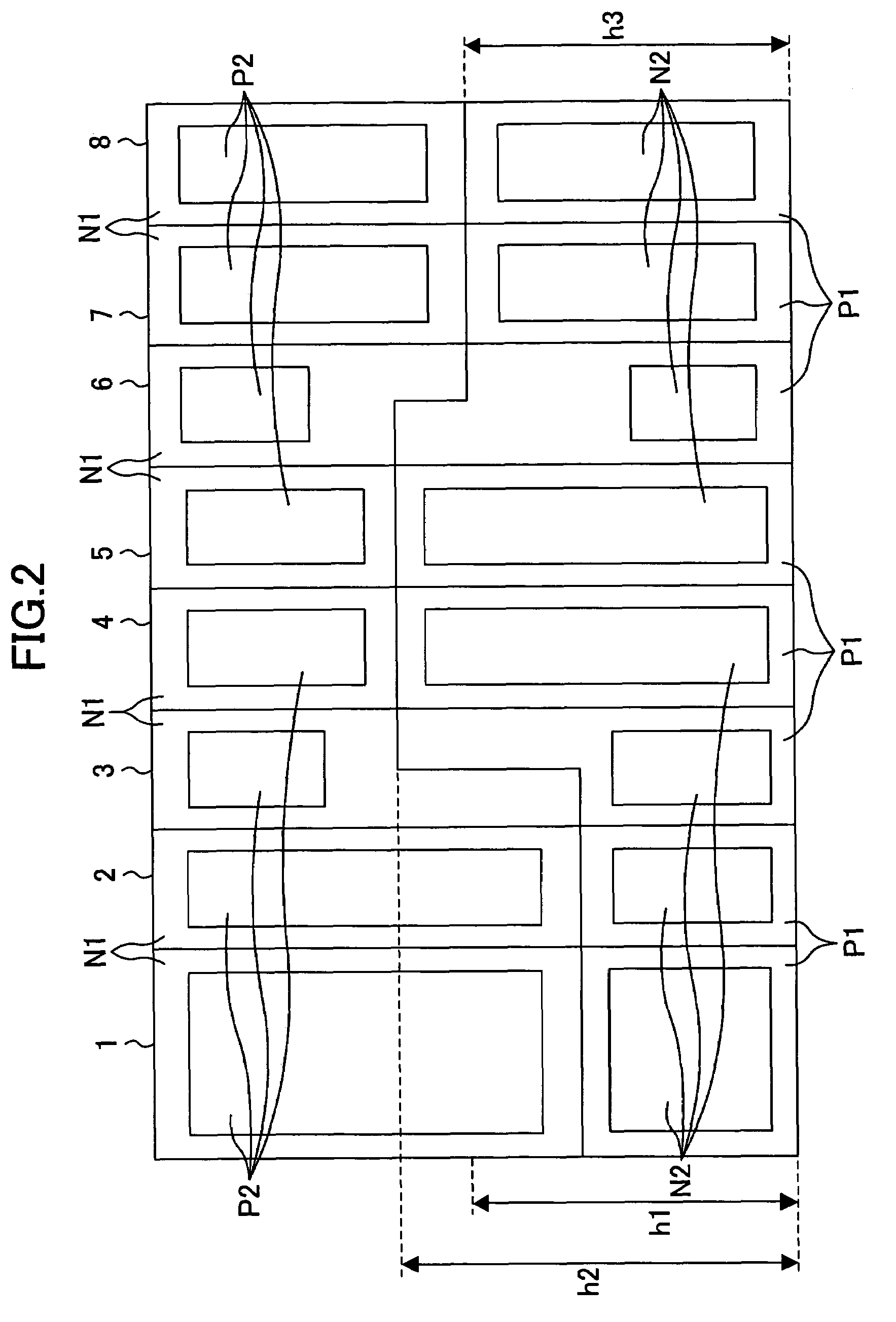
[0096]FIG. 3 is a flowchart illustrating a placing method for a semiconductor device according to a third example of the present invention. FIGS. 4 to 8 are diagrams illustrating a result of placement of standard cells based on the placing method of FIG. 3, and the standard cells. Hereinafter, the placing method of FIG. 3 will be described with reference to FIGS. 4 to 8.

[0097]In FIG. 3, S101 is a standard cell placing step of providing an initial placement in which standard cells having different well border line heights coexist.

[0098]FIG. 4 is a standard cell placement diagram illustrating a result of the placement in the standard cell placing step S101. Standard cells 104, 105, 108, 109, and 111 are each a standard cell (first standard cell) whose P-well region has a height h101 (first height). Standard cells 106, 107, and 110 are each a standard cell (second standard cell) whose P-well region has a height h102 (second height) which is different from the height h1.

[0099]At the tim...


PUM


Abstract

Of a plurality of standard cells in which an N-well region and a P-well region are vertically formed, some standard cells have a border line between the N-well region and the P-well region which is set to be a low height (first height), and other standard cells have a border line between the N-well region and the P-well region which is set to be a high height (second height), depending on the size of a transistor formed in the standard cell. Although these standard cells have different border lines, a standard cell for linking the border lines is provided. In such a standard cell, an empty space is created by forming a small-size transistor therein, and the empty space is utilized so that, for example, a left end of the border line is set to have the first height and a right end of the border line is set to have the second height, whereby the border line is converted so as to link the heights therein.

Description

CROSS REFERENCE TO RELATED APPLICATIONS[0001]This Non-provisional application claims priority under 35 U.S.C. § 119(a) on Patent Application No. 2004-366515 filed in Japan on Dec. 17, 2004 and Patent Application No. 2005-331926 filed in Japan on Nov. 16, 2005, the entire contents of which are hereby incorporated by reference.BACKGROUND OF THE INVENTION[0002]1. Field of the Invention[0003]The present invention relates to a standard cell, a standard cell library, a semiconductor device, and a placing method of the same.[0004]2. Description of the Related Art[0005]In conventional standard cell semiconductor devices, a number of standard cells are supposed to have substantially the same height so that they can be placed without a gap, i.e., with high density. Further, the cells have the same height of a border line between a P-well region and an N-well region (hereinafter referred to as a well border line height) so that an area efficiency of each individual standard cell is increased a...

Claims


Application Information

Patent Timeline
Patent Type & Authority Patents(United States)
IPC IPC(8): H01L27/10
CPCG06F17/5072H01L27/11807H01L27/0207G06F30/392
Inventor SHIMAMURA, AKIMITSU
Owner SOCIONEXT INC
Why Eureka
Try Eureka